

File:Atari 130XE DRAM U9-U16 and U26-U33 data bits (C070065 schematic).png

Summary
[edit | edit source]

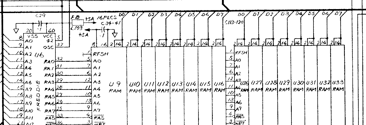
Detail of Atari's 130XE schematic: the main bank of 4164 DRAM, U9 (D0) to U16 (D7), and the extended bank, U26 (D0) to U33 (D7). Each chip's data in (pin 2) and data out (pin 14) are tied to one data bit; pin 8 is +5V and pin 16 ground, with one 0.1 µF decoupling capacitor per chip (C34-C41 and C113-C120).
Source
[edit | edit source]

Rendered from File:Atari 130XE Parts List and Production Test Instructions.pdf (Atari's 130XE Reference Manual), PDF page 14, the schematic diagram C070065 Rev. B drawn by Atari (Japan) Corporation in 1985, at the scan's 300 dpi, and cropped.
Author
[edit | edit source]

Atari (Japan) Corporation for Atari Corp.
Licence
[edit | edit source]

Copyright Atari Corp. Hosted for preservation and repair reference, with the source cited.
File history
Click on a date/time to view the file as it appeared at that time.
| Date/Time | Thumbnail | Dimensions | User | Comment | |
|---|---|---|---|---|---|
| current | 11:40, 25 October 2026 | | 1,400 × 480 (31 KB) | Josh (talk | contribs) | Upload schematic detail for Atari 130XE repair guides |
You cannot overwrite this file.
File usage
The following page uses this file:
