

File:Atari 130XE FREDDIE, MMU, DRAM and oscillator (C070065 schematic).png

Summary
[edit | edit source]

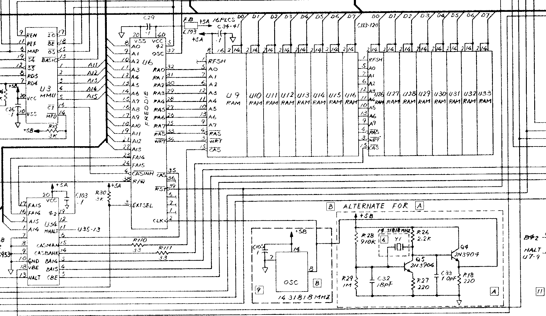
Detail of Atari's 130XE schematic: the MMU U3, FREDDIE U6 (RAS, CAS and write strobes and the multiplexed RAM address lines RA0-RA7, clock input CLK on pin 2, OSC on pin 37), the main DRAM U9-U16 and extended DRAM U26-U33, the extended-memory gate array U34 with its CASMAN and CASBANK outputs through R110 and R111, and the 14.31818 MHz oscillator: the crystal Y1 with Q4 and Q5, or the alternative oscillator module.
Source
[edit | edit source]

Rendered from File:Atari 130XE Parts List and Production Test Instructions.pdf (Atari's 130XE Reference Manual), PDF page 14, the schematic diagram C070065 Rev. B drawn by Atari (Japan) Corporation in 1985, at the scan's 300 dpi, and cropped.
Author
[edit | edit source]

Atari (Japan) Corporation for Atari Corp.
Licence
[edit | edit source]

Copyright Atari Corp. Hosted for preservation and repair reference, with the source cited.
File history
Click on a date/time to view the file as it appeared at that time.
| Date/Time | Thumbnail | Dimensions | User | Comment | |
|---|---|---|---|---|---|
| current | 11:40, 25 October 2026 | | 1,850 × 1,070 (79 KB) | Josh (talk | contribs) | Upload schematic detail for Atari 130XE repair guides |
You cannot overwrite this file.
File usage
The following page uses this file:
