
File:Atari 130XE board layout (C070067).png
Summary
[edit | edit source]

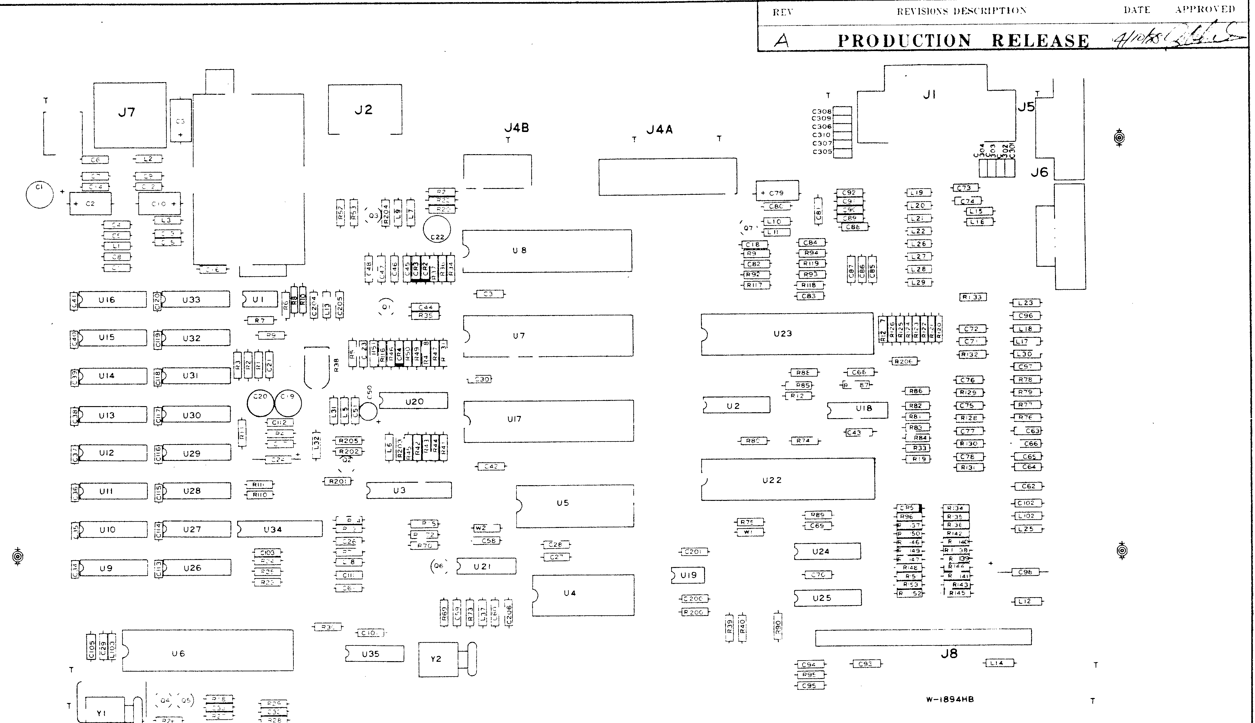
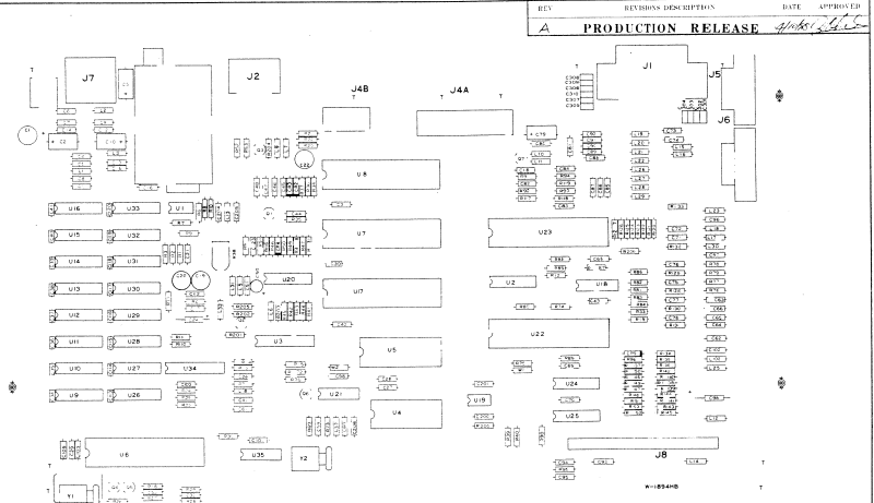
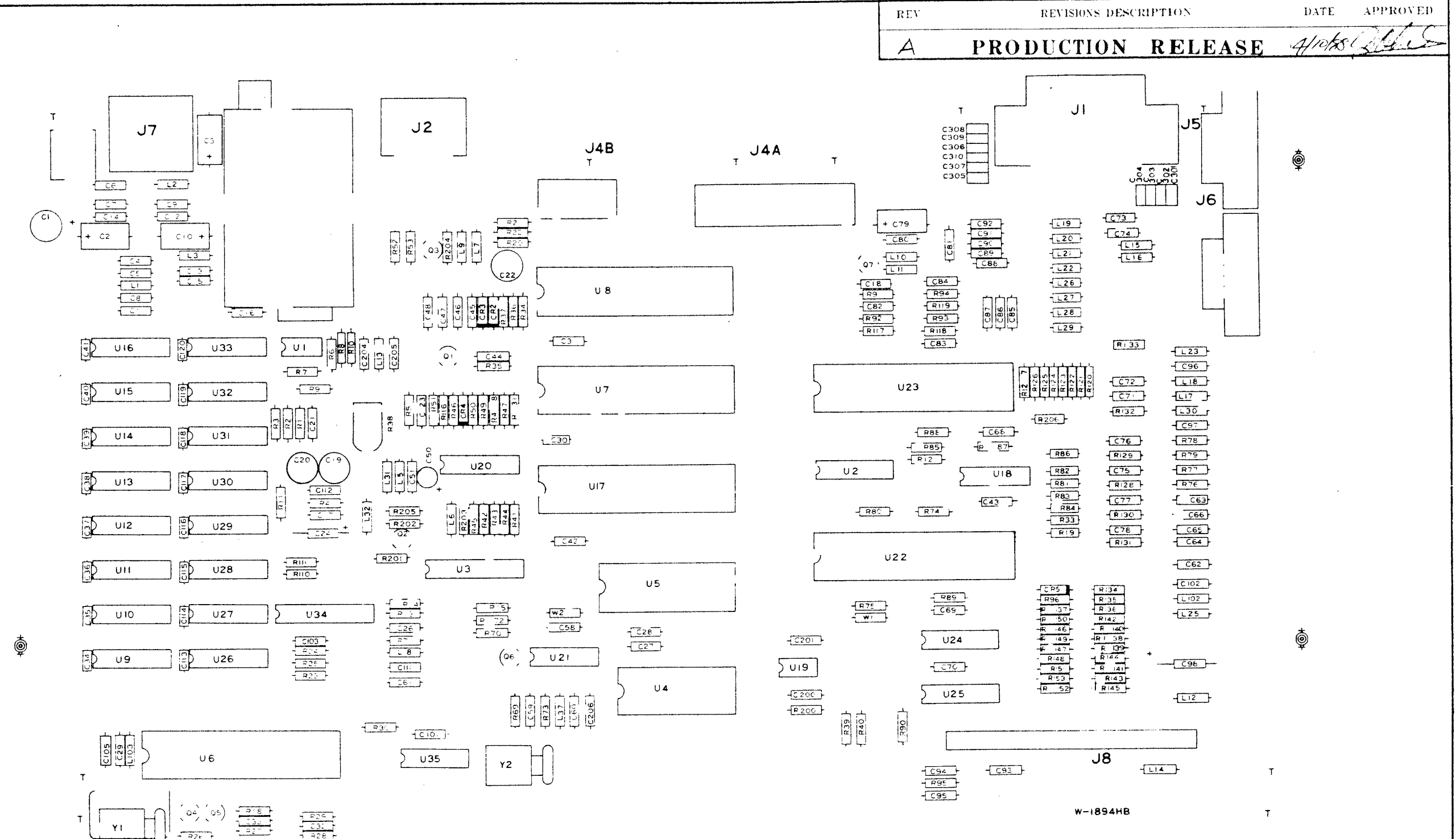
Atari's silk-screen drawing of the 130XE main board (drawing C070067 Rev. A), showing every component position: the DRAM in two columns at the left (U9-U16 and U26-U33), the CPU U8, ANTIC U7, GTIA U17, PIA U23 and POKEY U22 across the middle, the keyboard connector J8 at the front, and the rear connectors J7, J2, J4A/J4B, J1, J5 and J6.
Source
[edit | edit source]

Rendered from File:Atari 130XE Parts List and Production Test Instructions.pdf (Atari's 130XE Reference Manual), PDF page 12, drawing C070067 Rev. A, P.C.B., sheet 1 of 5 (silk print), dated April 1985, at the scan's 300 dpi, and cropped.
Author
[edit | edit source]

Atari (Japan) Corporation for Atari Corp.
Licence
[edit | edit source]

Copyright Atari Corp. Hosted for preservation and repair reference, with the source cited.
File history
Click on a date/time to view the file as it appeared at that time.
| Date/Time | Thumbnail | Dimensions | User | Comment | |
|---|---|---|---|---|---|
| current | 11:40, 25 October 2026 | | 4,080 × 2,350 (150 KB) | Josh (talk | contribs) | Upload schematic detail for Atari 130XE repair guides |
You cannot overwrite this file.
File usage
There are no pages that use this file.
