

File:Atari 130XE service check locations (Sams CC16).png

Summary
[edit | edit source]

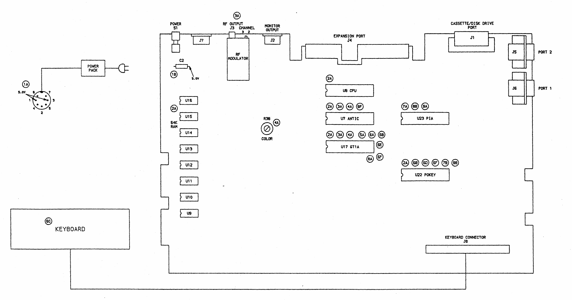
Sams' interconnecting diagram for the Atari 130XE from Computerfacts CC16, preliminary service checks (page VII): the main board outline with S1, J7, C2 (5.0 V), the RF modulator, J2, J4, J1, J5, J6, the 64K RAM U9-U16, the colour control R38, the CPU U8, ANTIC U7, GTIA U17, PIA U23, POKEY U22 and the keyboard connector J8, each marked with the numbers of the service checks that apply to it. Pins 1 and 3 of the power pack plug are marked 5.0 V.
Source
[edit | edit source]

Cropped from File:Sams Computerfacts Atari 130XE (CC16).pdf, PDF page 19, rendered at 200 dpi.
Author
[edit | edit source]

Howard W. Sams & Co.
Licence
[edit | edit source]

Copyright Howard W. Sams & Co. Not freely licensed. Hosted for preservation and repair reference, with the source cited.
File history
Click on a date/time to view the file as it appeared at that time.
| Date/Time | Thumbnail | Dimensions | User | Comment | |
|---|---|---|---|---|---|
| current | 11:40, 25 October 2026 | | 1,880 × 986 (93 KB) | Josh (talk | contribs) | Upload Sams detail for Atari 130XE repair guides |
You cannot overwrite this file.
File usage
The following 2 pages use this file:
