

File:Atari 800XL DRAM U9-U16 data bits (FD100740 schematic).png

Summary
[edit | edit source]

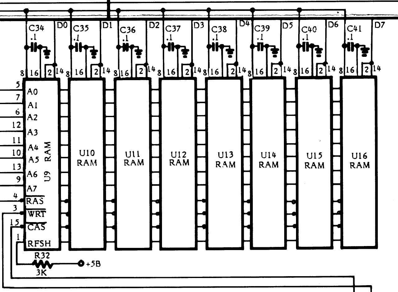
Detail of the 800XL schematic in Atari's 800XL Computer Field Service Manual (FD100740 Rev. 01, February 1984), section 5: the eight 64K × 1 dynamic RAMs U9-U16. Each chip's data in (pin 2) and data out (pin 14) are joined to one data line, U9 to D0 through U16 to D7. Pin 8 is the supply, pin 16 ground, with a 0.1 µF decoupling capacitor (C34-C41) at each chip; address inputs A0-A7 are on pins 5, 7, 6, 12, 11, 10, 13 and 9, RAS on pin 4, WRT on pin 3, CAS on pin 15, and pin 1 is pulled up to +5B through R32 (3 kΩ).
Source
[edit | edit source]

Rendered from File:Atari 800XL Computer Field Service Manual FD100740 Rev 01.pdf, PDF page 36, at 300 dpi and cropped.
Author
[edit | edit source]

Atari, Inc.
Licence
[edit | edit source]

Copyright Atari, Inc. Hosted for preservation and repair reference, with the source cited.
File history
Click on a date/time to view the file as it appeared at that time.
| Date/Time | Thumbnail | Dimensions | User | Comment | |
|---|---|---|---|---|---|
| current | 10:55, 25 October 2026 | | 1,280 × 940 (68 KB) | Josh (talk | contribs) | Upload for repair guide |
You cannot overwrite this file.
File usage
The following page uses this file:
