

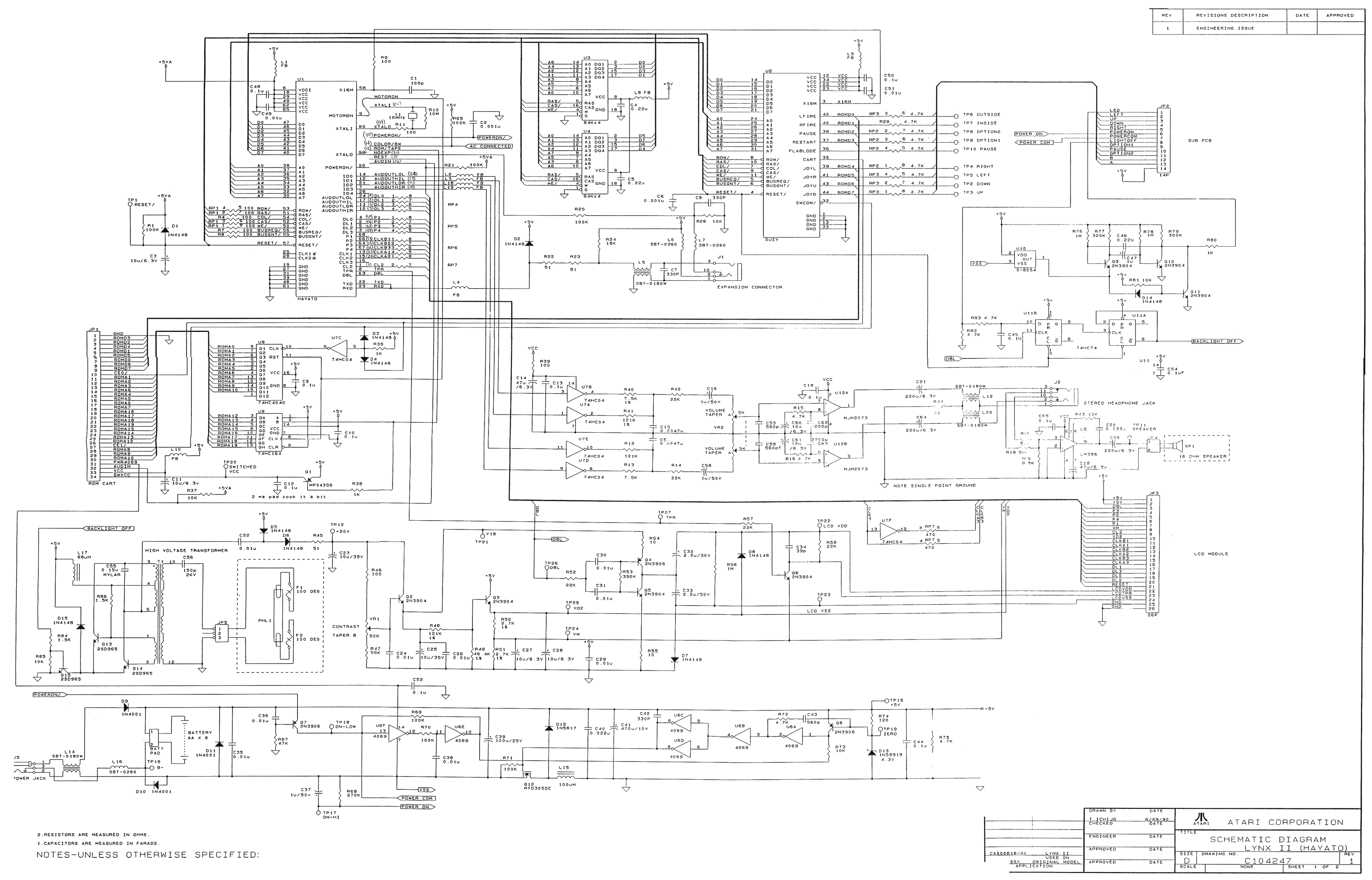
File:Atari Lynx II schematic C104247 Rev 1.png

Summary
[edit | edit source]

Atari Corporation schematic diagram "Lynx II (Hayato)", drawing C104247, revision 1 (engineering issue), sheet 1: the Lynx II main board with the Hayato chip (U1) in place of Mikey, Suzy (U2), two 64K × 4 DRAMs, the cartridge connector, the backlight high-voltage transformer and on/off circuit, the stereo audio stage with its 16 Ω speaker, and the 9 V power input and regulator circuit. The title block is dated 29 June 1990.
Source
[edit | edit source]

Console5 TechWiki, https://wiki.console5.com/wiki/File:Atari-Lynx-II-Schematic-(Hayato)-C104247-6-29-90.png (retrieved 2026-10-01). A PDF of the same drawing is on archive.org as "Schematic Diagram Lynx II Hayto (1992)(U)".

Author
[edit | edit source]

Atari Corporation.
Licence
[edit | edit source]

Copyright Atari Corporation. Not freely licensed. Hosted for preservation and repair reference.
File history
Click on a date/time to view the file as it appeared at that time.
| Date/Time | Thumbnail | Dimensions | User | Comment | |
|---|---|---|---|---|---|
| current | 00:38, 1 October 2026 | | 3,104 × 1,991 (272 KB) | Josh (talk | contribs) | Atari Lynx II (Hayato) schematic C104247 Rev 1 (via Console5 TechWiki) |
You cannot overwrite this file.
File usage
The following page uses this file:
