

File:Burnt PCB laminate repair cross-section (diagram).png

Summary
[edit | edit source]

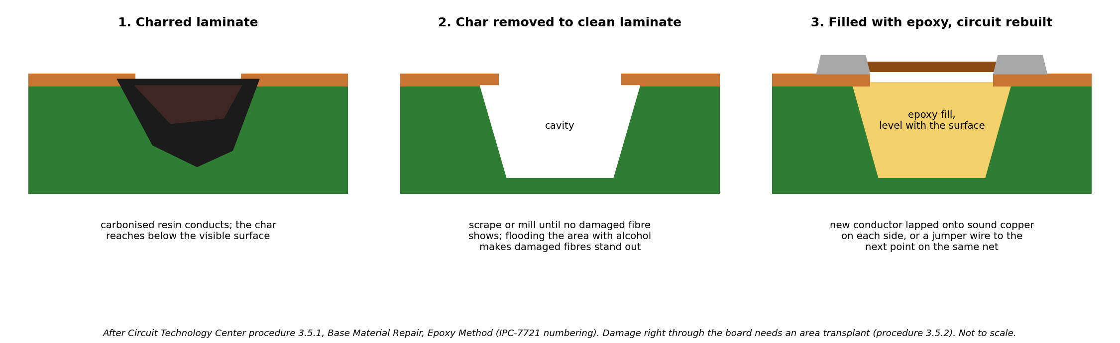
Three cross-sections of a burnt area of circuit board: (1) carbonised laminate under a burnt trace, extending below the visible surface; (2) the char scraped or milled out to clean laminate; (3) the cavity filled level with epoxy and the circuit rebuilt with a new conductor lapped onto sound copper on each side. Not to scale.
Source
[edit | edit source]

Drawn for this wiki (2026-10-25), following Circuit Technology Center, procedure 3.5.1, Base Material Repair, Epoxy Method and procedure 3.5.2, Base Material Repair, Area Transplant Method.
Author
[edit | edit source]

RetroTechCollection wiki.
Licence
[edit | edit source]

Drawn for this wiki and released under Creative Commons Attribution-ShareAlike 4.0.
File history
Click on a date/time to view the file as it appeared at that time.
| Date/Time | Thumbnail | Dimensions | User | Comment | |
|---|---|---|---|---|---|
| current | 14:49, 25 October 2026 | | 2,250 × 690 (104 KB) | Josh (talk | contribs) | Upload for the PCB repair technique pages |
You cannot overwrite this file.
File usage
The following page uses this file:
