

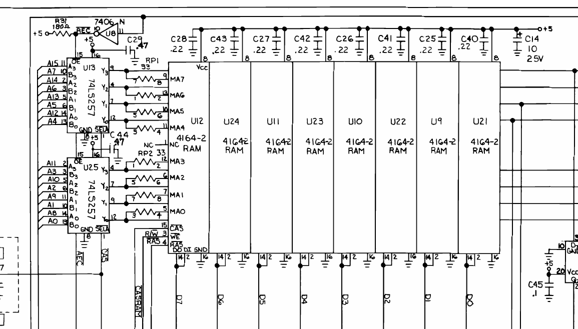
File:C64 schematic 326106 sheet 2 main RAM and data bits.png

Summary
[edit | edit source]

Detail of Commodore schematic 326106, sheet 2 of 2, for the original Commodore 64 board (assembly 326298), as printed on page 22 of the Service Manual C64/C64C (PN-314001-03, March 1992). It shows the eight 4164 RAM chips in the order U12, U24, U11, U23, U10, U22, U9, U21 with their data lines D7 to D0 (pins 2 and 14 joined), the shared +5 V on pin 8 and ground on pin 16, the decoupling capacitors C25-C28 and C40-C43 (0.22 µF) and C14 (10 µF 25 V), the 74LS257 address multiplexers U13 and U25 with resistor packs RP1 and RP2, and the CASRAM, R/W and RAS lines.
Source
[edit | edit source]

Rendered from File:Commodore 64 - 64C Service Manual.pdf, PDF page 28 (manual page 22), at 200 dpi and cropped.
Author
[edit | edit source]

Commodore Business Machines.
Licence
[edit | edit source]

Copyright Commodore Business Machines. Hosted for preservation and repair reference, with the source cited.
File history
Click on a date/time to view the file as it appeared at that time.
| Date/Time | Thumbnail | Dimensions | User | Comment | |
|---|---|---|---|---|---|
| current | 08:57, 25 October 2026 | | 1,155 × 658 (76 KB) | Josh (talk | contribs) | Upload for Commodore 64 RAM Replacement guide |
You cannot overwrite this file.
File usage
The following page uses this file:
