

File:NES-001 video buffer Q1 and R2 (Schenk redraw).png
Size of this preview: 709 × 417 pixels.
Original file (709 × 417 pixels, file size: 47 KB, MIME type: image/png)
Summary
[edit | edit source]

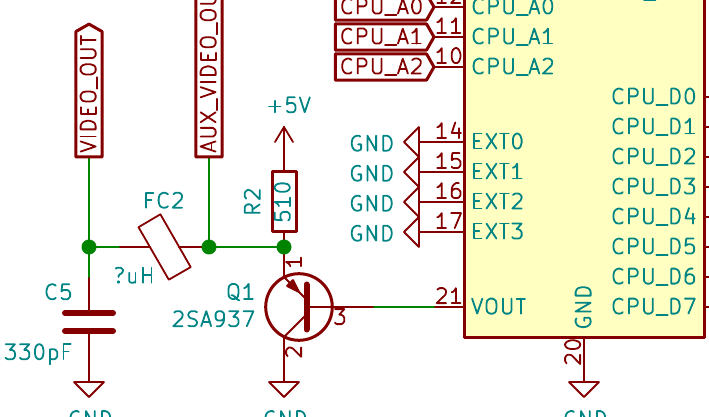
The video output section of a 2020 redrawn NES-001 schematic: the PPU's VOUT on pin 21 drives the base of Q1 (2SA937), whose emitter is pulled up to +5 V by R2 (510 ohms) and feeds VIDEO_OUT through FC2 and the AUX_VIDEO_OUT line, with C5 330 pF to ground.
Source
[edit | edit source]

Cropped for this wiki from File:NES-001.pdf, N. Schenk (Schenktronics), NES Schematics, file Original_NES.sch, rev. 1.0, 2020-06-05 (described on NES-001 Schematic).
Author
[edit | edit source]

N. Schenk (Schenktronics)
Licence
[edit | edit source]

No licence is stated on the drawing. The circuit design is Nintendo's. Hosted for repair reference with the source cited.
File history
Click on a date/time to view the file as it appeared at that time.
| Date/Time | Thumbnail | Dimensions | User | Comment | |
|---|---|---|---|---|---|
| current | 09:03, 25 October 2026 | | 709 × 417 (47 KB) | Josh (talk | contribs) | Upload for NES repair guides; source and licence on the description page |
You cannot overwrite this file.
File usage
The following page uses this file:
