

File:PCB trace repair lap joint (diagram).png

Summary
[edit | edit source]

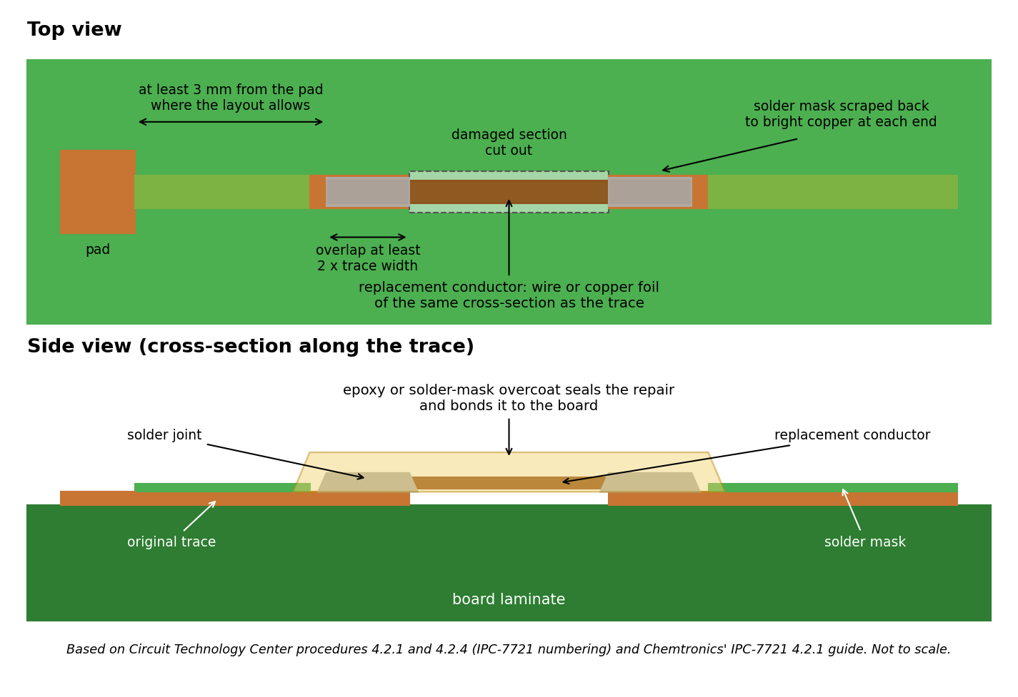
Diagram of a broken printed-circuit trace repaired with a replacement conductor, in top view and in section. The damaged section is cut out, the solder mask is scraped back at each end, the new wire or copper foil overlaps each end of the trace by at least twice the trace width, the joints are kept at least 3 mm from the nearest pad where the layout allows, and the repair is coated with epoxy or solder mask. Not to scale.
Source
[edit | edit source]

Drawn for this wiki (2026-10-25). The dimensions are from Circuit Technology Center, procedure 4.2.1, Conductor Repair, Foil Jumper, Epoxy Method and procedure 4.2.4, Conductor Repair, Surface Wire Method, and Chemtronics, "HOW-TO: PCB Trace Repair Using Foil Jumper & Epoxy Overcoat" (based on IPC-7721 4.2.1).
Author
[edit | edit source]

RetroTechCollection wiki.
Licence
[edit | edit source]

Drawn for this wiki and released under Creative Commons Attribution-ShareAlike 4.0.
File history
Click on a date/time to view the file as it appeared at that time.
| Date/Time | Thumbnail | Dimensions | User | Comment | |
|---|---|---|---|---|---|
| current | 14:49, 25 October 2026 | | 1,425 × 977 (120 KB) | Josh (talk | contribs) | Upload for the PCB repair technique pages |
You cannot overwrite this file.
File usage
The following page uses this file:
