

File:SGI POWER Series system diagram (Technical Report 1989 Figure 1).png

Summary
[edit | edit source]

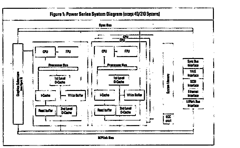
Figure 1, "Power Series System Diagram (except 4D/210 Systems)", from Silicon Graphics' POWER Series Technical Report (1989), page 4. Block diagram of the POWERpath architecture: two of the CPU and FPU pairs with their processor bus, first-level instruction and data caches, read and write buffers and second-level data cache; the Sync Bus and MPlink bus; system memory with its ECC controller; the graphics subsystem; and the Sync Bus, VME, SCSI, Ethernet and MPlink interfaces. Rendered from the scanned PDF at 200 dpi and cropped to the figure. See SGI Power Series.
Source
[edit | edit source]

File:SGI POWER Series Technical Report (1989).pdf, page 4. That PDF came from the Internet Archive item sgi-power-series-technical-report-1989.
Author
[edit | edit source]

Silicon Graphics, Inc.
Licence
[edit | edit source]

Copyright 1989 Silicon Graphics, Inc. Hosted for preservation and repair reference, with the source cited.
File history
Click on a date/time to view the file as it appeared at that time.
| Date/Time | Thumbnail | Dimensions | User | Comment | |
|---|---|---|---|---|---|
| current | 01:14, 22 October 2026 | | 984 × 607 (16 KB) | Josh (talk | contribs) | Figure 1 from the SGI POWER Series Technical Report (1989) |
You cannot overwrite this file.
File usage
The following 2 pages use this file:
