

File:SNES video encoder and output buffers (Donaldson redraw).png

Summary
[edit | edit source]

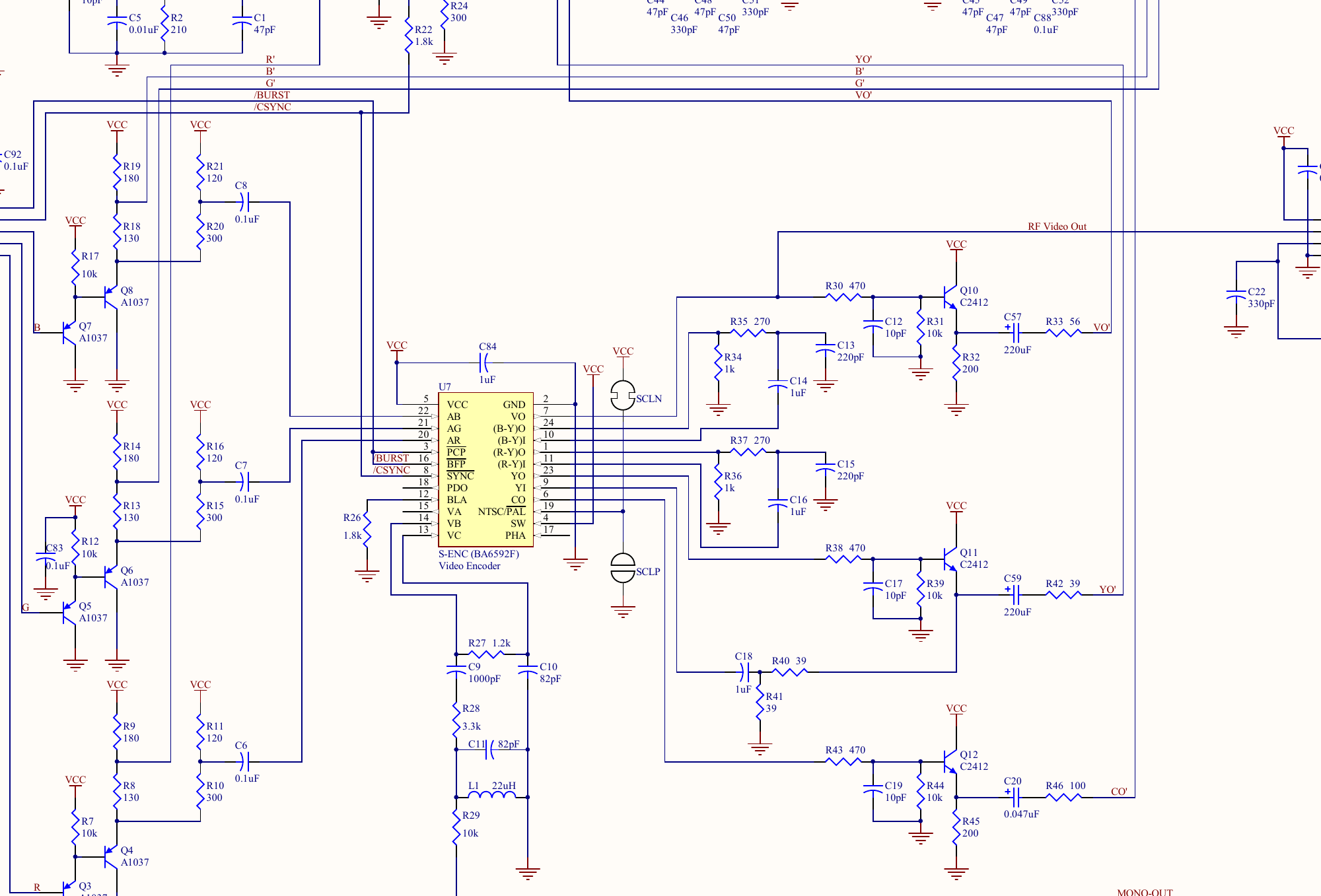
Crop of the video output section of Jonathon W. Donaldson's community redraw of the NTSC Super NES main board (SNS-CPU-GPM-01/02 and SNS-CPU-RGB-01/02), revision 1.5, 24 February 2014. At the left, the PPU2's red, green and blue outputs (R, G, B) pass through 2SA1037 transistor pairs (Q3 and Q4 red, Q5 and Q6 green, Q7 and Q8 blue) to the RGB outputs R', G' and B', and through 0.1 uF capacitors C6, C7 and C8 to the AR, AG and AB inputs (pins 20, 21, 22) of the video encoder U7, drawn as an S-ENC (BA6592F). The encoder's colour-difference signals pass through filters including C14 and C16 (1 uF) between its (B-Y) and (R-Y) outputs and inputs. At the right, 2SC2412 buffers drive the composite output (Q10, C57 220 uF, R33 56 ohm, VO', also the RF video feed), the S-Video luminance output (Q11, C59 220 uF, R42 39 ohm, YO') and the S-Video chroma output (Q12, C20 0.047 uF, R46 100 ohm, CO'). Not a Nintendo document.
Source
[edit | edit source]

Cropped from File:Snes schematic.pdf, described on SNES Schematic. Rendered at 450 dpi.
Author
[edit | edit source]

Jonathon W. Donaldson (redraw). The circuit is Nintendo's.
Licence
[edit | edit source]

No licence accompanies the drawing. Hosted for repair reference.
File history
Click on a date/time to view the file as it appeared at that time.
| Date/Time | Thumbnail | Dimensions | User | Comment | |
|---|---|---|---|---|---|
| current | 11:01, 25 October 2026 | | 2,000 × 1,357 (212 KB) | Josh (talk | contribs) | Upload for SNES repair guide |
You cannot overwrite this file.
File usage
The following page uses this file:
