

File:SNS-CPU-1CHIP-02 power section (Evan-Amos).jpg
Size of this preview: 656 × 600 pixels. Other resolution: 1,320 × 1,207 pixels.
Original file (1,320 × 1,207 pixels, file size: 346 KB, MIME type: image/jpeg)
Summary
[edit | edit source]

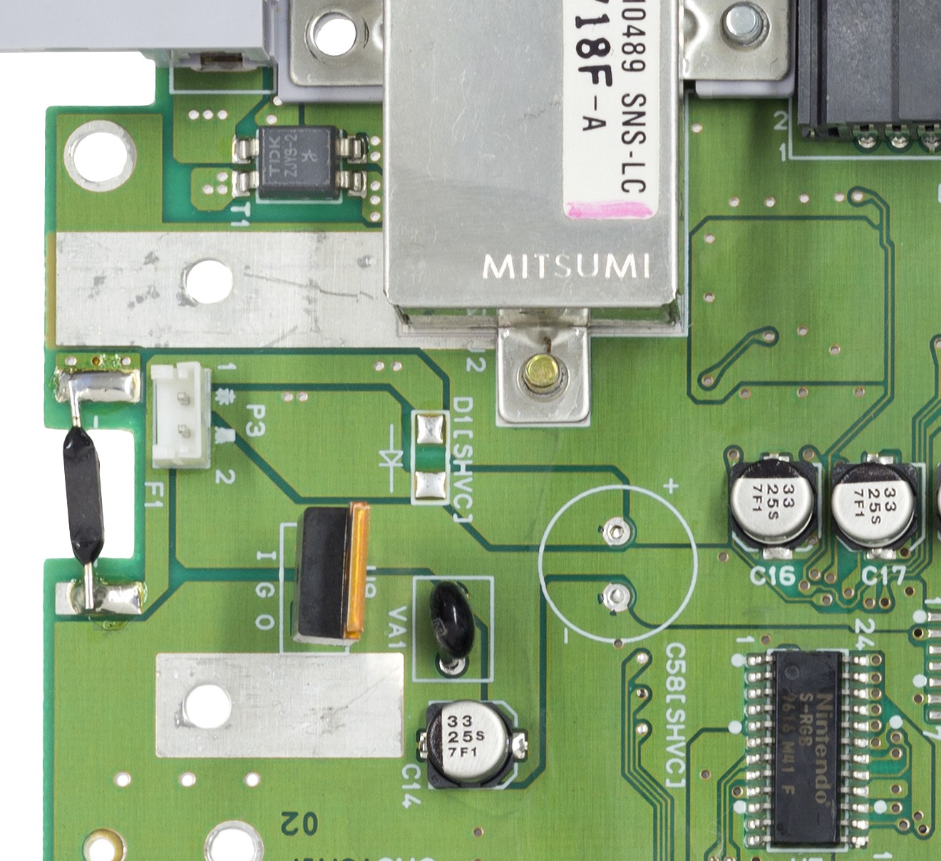
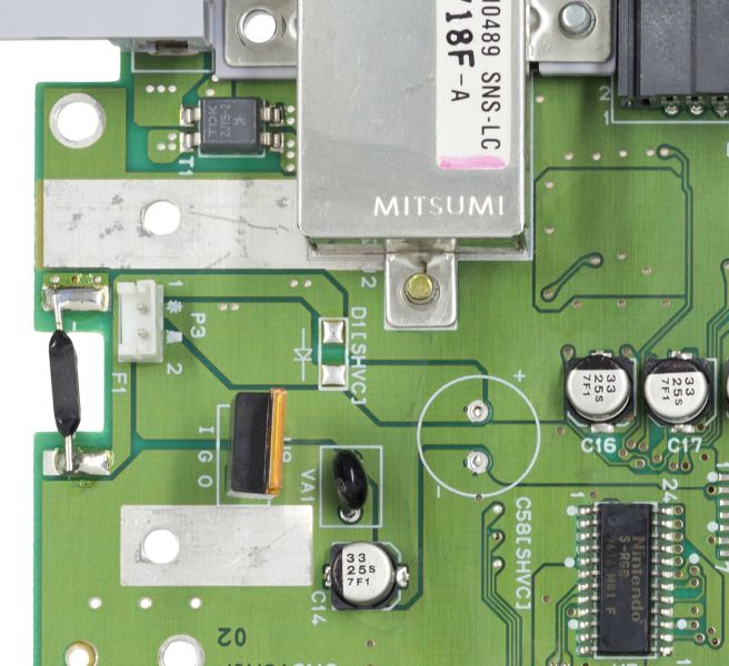
Crop of the top of a North American SNS-CPU-1CHIP-02 Super NES main board around the power input: line filter T1 (TDK ZJYS-2), the axial fuse F1, power-switch connector P3, the regulator, with its heatsink removed, beside the silkscreen I, G and O, surge absorber VA1, the 33 uF 25 V capacitor C14, the empty positions D1 and C58 marked [SHVC], and the S-RGB video encoder at the right.
Source
[edit | edit source]

Cropped from Super-Nintendo-1Chip-Motherboard-Top-Flat.jpg on Wikimedia Commons (retrieved 2026-10-25).

Author
[edit | edit source]

Evan-Amos.
Licence
[edit | edit source]

Public domain, as released by the author on Wikimedia Commons.
File history
Click on a date/time to view the file as it appeared at that time.
| Date/Time | Thumbnail | Dimensions | User | Comment | |
|---|---|---|---|---|---|
| current | 10:46, 25 October 2026 | | 1,320 × 1,207 (346 KB) | Josh (talk | contribs) | Upload for SNES repair guide |
You cannot overwrite this file.
File usage
The following page uses this file:
