

File:Sega Master System II power circuit area.jpg

Summary
[edit | edit source]

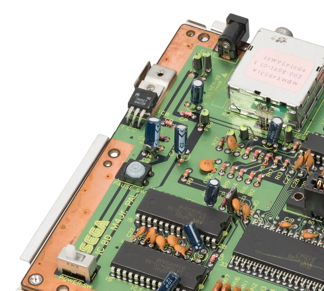
Crop of Evan-Amos's photograph of a Sega Master System II PAL main board (IC BD M4Jr. PAL), showing the power section: the DC jack at the top, the 7805 regulator IC8 on its heat sink at the left edge with the pins marked I, C and O, diode D2, the capacitors C41, C42 and C43, bead FB3, the RF modulator (200-5091-01), the pause switch and the slide power switch at the bottom left.
Source
[edit | edit source]

Cropped from File:Sega-Master-System-MkII-Black-Motherboard-1.jpg, which is from Wikimedia Commons, File:Sega-Master-System-MkII-Black-Motherboard-1.jpg. Nothing else changed.


Author
[edit | edit source]

Evan-Amos
Licence
[edit | edit source]

Public domain, as released by the author on Wikimedia Commons.
File history
Click on a date/time to view the file as it appeared at that time.
| Date/Time | Thumbnail | Dimensions | User | Comment | |
|---|---|---|---|---|---|
| current | 11:12, 25 October 2026 | | 1,100 × 986 (269 KB) | Josh (talk | contribs) | Upload for Master System II repair guides |
You cannot overwrite this file.
File usage
The following page uses this file:
