

File:Sega Master System II power input schematic.png

Summary
[edit | edit source]

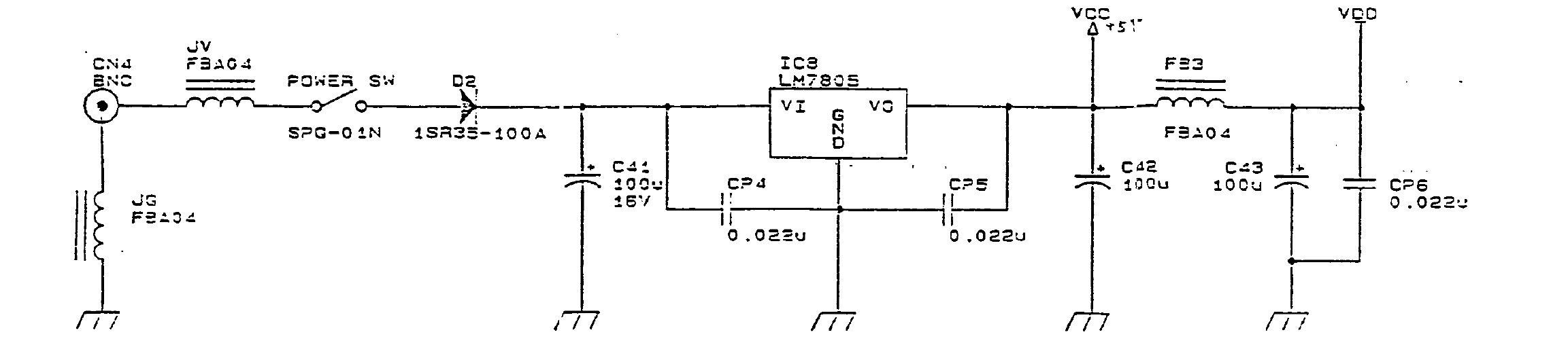
Crop of the power input section of Sega's Sega Master System II PAL schematic, sheet 1: CN4 (DC input), bead JV, the power switch (SPG-01N), diode D2 (1SR35-100A), C41 (100 µF 16 V) and CP4 (0.022 µF) on the input of IC8 (drawn as an LM7805), CP5 (0.022 µF) and C42 (100 µF) on its output (Vcc, +5 V), then bead FB3 to VDD with C43 (100 µF) and CP6 (0.022 µF), and bead JG in the ground return.
Source
[edit | edit source]

Sega Enterprises, Ltd., Sega Master System II Service Manual, April 1991, schematic diagram for the PAL version, "IC BD M4JR PAL" 171-5922A, sheet 1 of 3 (p. 11, PDF p. 18), hosted on this wiki as File:Sega Master System II Service Manual April 1991.pdf. Cropped and converted to greyscale; nothing else changed.
Author
[edit | edit source]

Sega Enterprises, Ltd.
Licence
[edit | edit source]

Copyright Sega Enterprises, Ltd. Hosted for preservation and repair reference, with the source cited.
File history
Click on a date/time to view the file as it appeared at that time.
| Date/Time | Thumbnail | Dimensions | User | Comment | |
|---|---|---|---|---|---|
| current | 11:12, 25 October 2026 | | 2,305 × 505 (18 KB) | Josh (talk | contribs) | Upload for Master System II repair guides |
You cannot overwrite this file.
File usage
The following page uses this file:
