

File:Sega Master System II video output schematic.png

Summary
[edit | edit source]

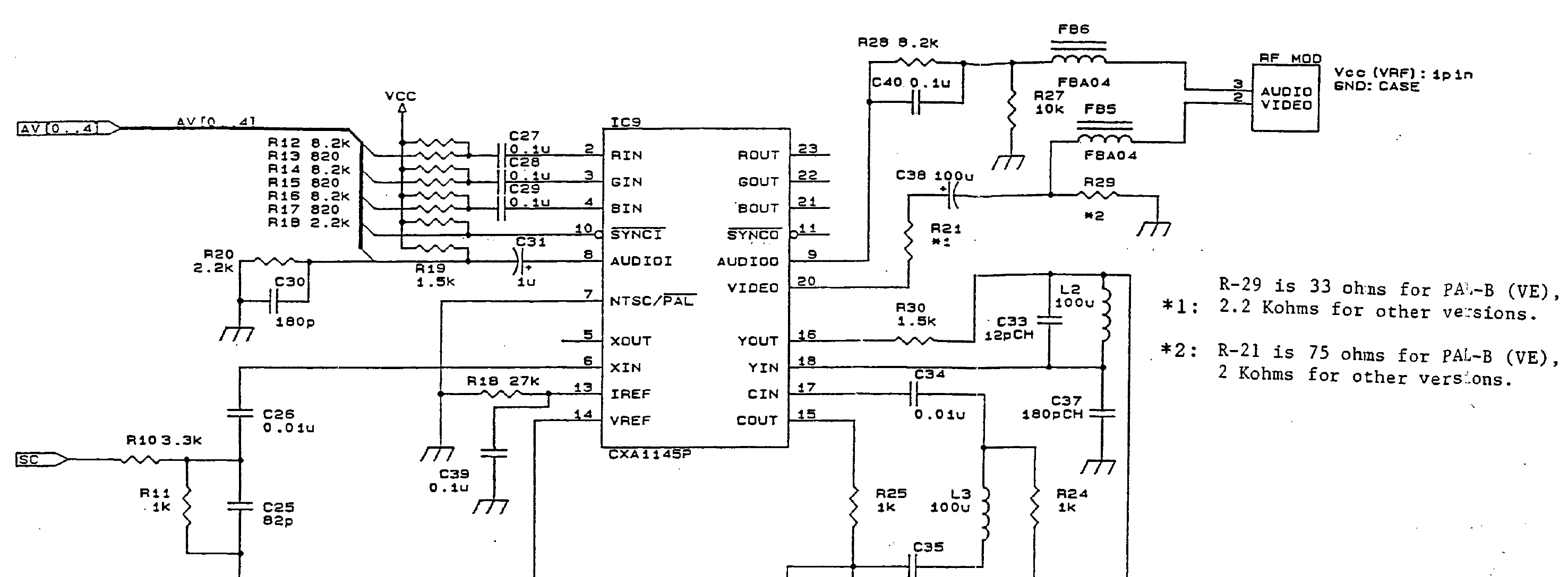
Crop of the video encoder section of Sega's Sega Master System II PAL schematic, sheet 3: IC9 (CXA1145P) with its RGB inputs on pins 2, 3 and 4, composite video out on pin 20 through R21, C38 (100 µF) and bead FB5 to the RF modulator video input (pin 2), R29 from the modulator side of C38 to ground, audio out on pin 9 through R28 and FB6 to modulator pin 3, and Sega's notes on the PAL-B (VE) values of R21 and R29.
Source
[edit | edit source]

Sega Enterprises, Ltd., Sega Master System II Service Manual, April 1991, schematic diagram for the PAL version, "IC BD M4JR PAL" 171-5922A, sheet 3 of 3 (p. 13, PDF p. 20), hosted on this wiki as File:Sega Master System II Service Manual April 1991.pdf. Cropped and converted to greyscale; nothing else changed.
Author
[edit | edit source]

Sega Enterprises, Ltd.
Licence
[edit | edit source]

Copyright Sega Enterprises, Ltd. Hosted for preservation and repair reference, with the source cited.
File history
Click on a date/time to view the file as it appeared at that time.
| Date/Time | Thumbnail | Dimensions | User | Comment | |
|---|---|---|---|---|---|
| current | 11:12, 25 October 2026 | | 2,953 × 1,088 (60 KB) | Josh (talk | contribs) | Upload for Master System II repair guides |
You cannot overwrite this file.
File usage
The following page uses this file:
