

File:Sega Mega CD sub board power input schematic.png
Summary
[edit | edit source]

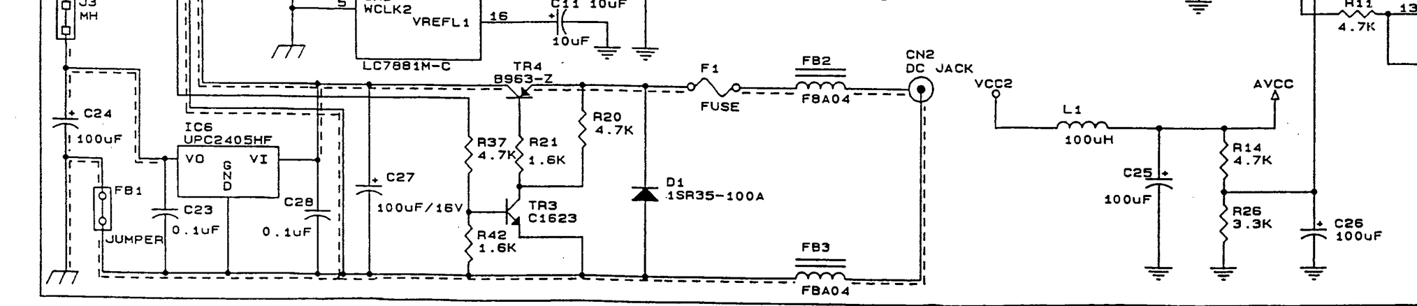
The power input section of Sega's schematic for the Mega-CD (Sega CD Model 1) sub board, "PC BD MEGA-CD SUB BD", assembly 837-8046-01, drawing 171-6115C rev. C: DC jack CN2, ferrite beads FB2 and FB3, fuse F1, diode D1 (1SR35-100A), transistors TR4 (B963-Z) and TR3 (C1623), C27, regulator IC6 (µPC2405HF), the VCC2 output and L1 to AVCC. Cropped from the schematic page of the export maintenance manual.
Source
[edit | edit source]

Sega Enterprises, Ltd., MEGA-CD Maintenance Manual (Export), August 1992, Rev. A, section 9, sub board schematic, PDF page 105. Hosted on this wiki as File:Sega CD Service Manual.pdf; see Sega CD Service Manual.
Author
[edit | edit source]

Sega Enterprises, Ltd.
Licence
[edit | edit source]

Copyright Sega Enterprises, Ltd. Hosted for preservation and repair reference, with the source cited.
File history
Click on a date/time to view the file as it appeared at that time.
| Date/Time | Thumbnail | Dimensions | User | Comment | |
|---|---|---|---|---|---|
| current | 10:38, 25 October 2026 | | 2,028 × 438 (110 KB) | Josh (talk | contribs) | Upload for repair guide |
You cannot overwrite this file.
File usage
The following page uses this file:
