

File:Sega SG-1000 main board (later layout).jpg

Summary
[edit | edit source]

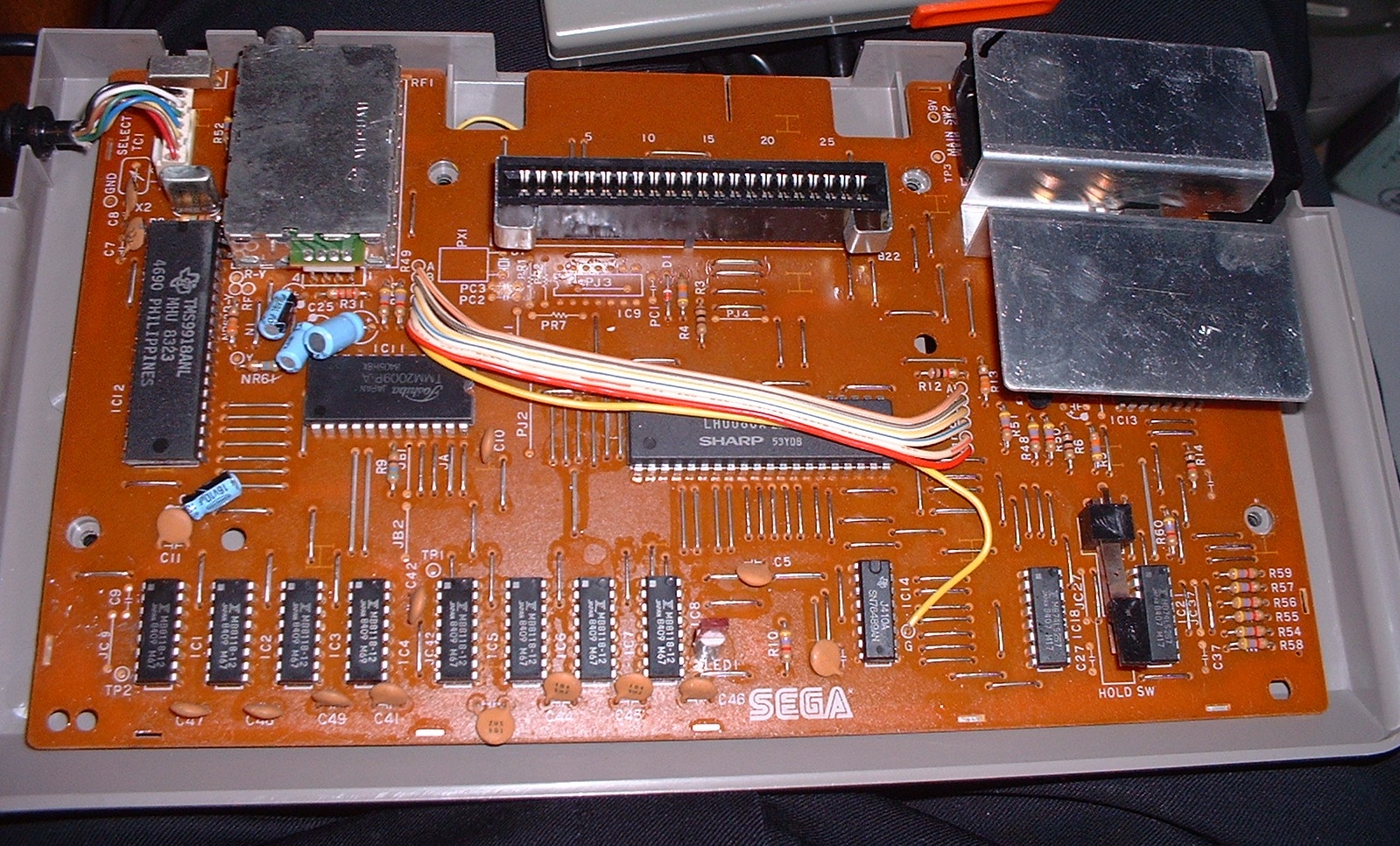
An SG-1000 main board of the later layout in the lower case: Sharp LH0080A CPU, TMS9918ANL video chip at IC12, TMM2009P-A work RAM at IC11, SN76489AN sound chip at IC14, eight MB8118-12 video RAMs at IC1 to IC8 with ceramic capacitors C41 to C49, the RF modulator can at top left, the cartridge connector, and the regulator under its heat sink at top right beside MAIN SW2, with a pad marked 9V and test point TP3. The electrolytic at C25 is beside the RF modulator.
Source
[edit | edit source]

MSX Wiki, https://www.msx.org/wiki/File:Sega_SG-1000-v2-PCB.jpg (retrieved 2026-10-19), used on the MSX Wiki's "Sega SG-1000" page as "Sega SG-1000 v2 PCB".

Author
[edit | edit source]

Uploaded to the MSX Wiki by user Gdx (10 September 2020), cropped version uploaded by Mars2000you (12 February 2026); photographer not recorded.
Licence
[edit | edit source]

No licence is given on the source page. Hosted here, credited to its source, to identify the board and its parts for repair reference.
File history
Click on a date/time to view the file as it appeared at that time.
| Date/Time | Thumbnail | Dimensions | User | Comment | |
|---|---|---|---|---|---|
| current | 22:09, 19 October 2026 | | 1,599 × 966 (674 KB) | Josh (talk | contribs) | Upload for the Sega SG-1000 pages |
You cannot overwrite this file.
File usage
The following 2 pages use this file:
