

File:Sony HB-55P HB-75P power board circuit (service manual).png
Size of this preview: 800 × 491 pixels. Other resolution: 2,473 × 1,518 pixels.

Original file (2,473 × 1,518 pixels, file size: 68 KB, MIME type: image/png)
Summary
[edit | edit source]

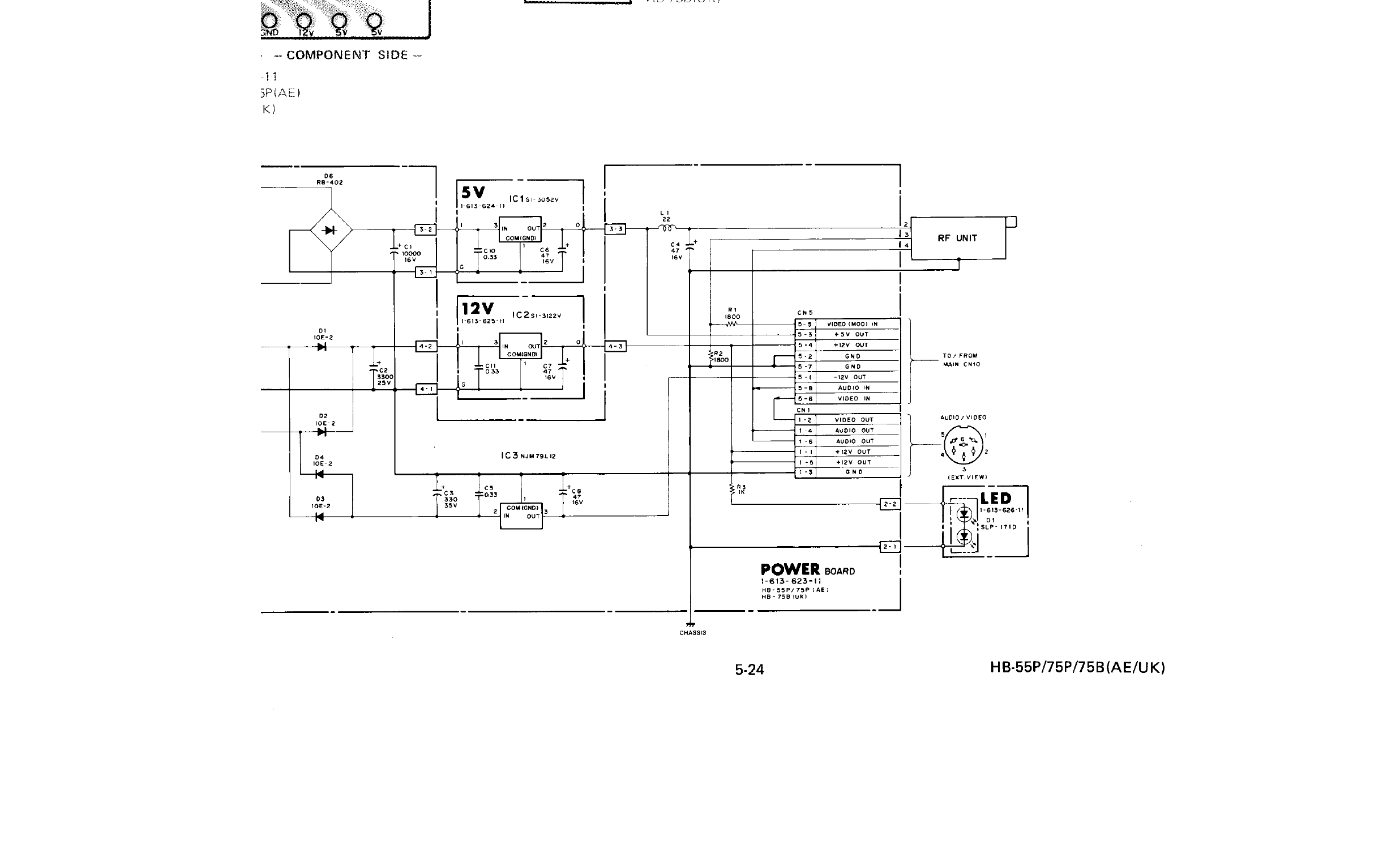
The power board section of Sony's HB-55P/75P/75B schematic (page 5-24): bridge rectifier D6 (RB-402) and reservoir C1 (10000 µF 16 V) feeding the 5 V board's SI-3052V (IC1); D1 and D2 with C2 (3300 µF 25 V) feeding the 12 V board's SI-3122V (IC2); D3 and D4 with C3 (330 µF 35 V) feeding the NJM79L12 (IC3) for −12 V; connectors CN5 to the main board and CN1, the 6-pin audio/video socket; the LED board.
Source
[edit | edit source]

Cropped from File:Sony HB-55P HB-75P HB-75B Service Manual.pdf, page 5-24.
Author
[edit | edit source]

Sony Corporation.
Licence
[edit | edit source]

Copyright Sony Corporation. Hosted for preservation and repair reference, with the source cited.
File history
Click on a date/time to view the file as it appeared at that time.
| Date/Time | Thumbnail | Dimensions | User | Comment | |
|---|---|---|---|---|---|
| current | 13:34, 21 October 2026 | | 2,473 × 1,518 (68 KB) | Josh (talk | contribs) | Upload for Sony HB-55 repair pages |
You cannot overwrite this file.
File usage
The following page uses this file:
