

File:Super NES controller circuit, single-IC version (Playtronic manual).png

Summary
[edit | edit source]

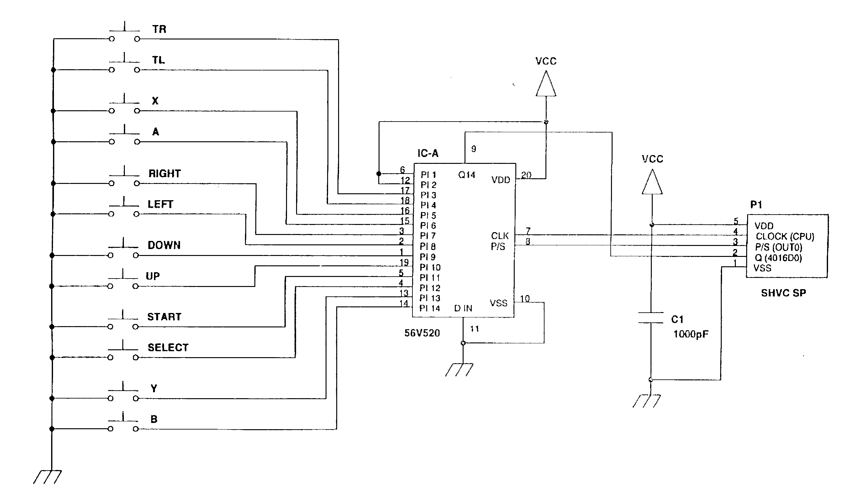
Circuit of the single-IC Super NES controller from Playtronic's Brazilian service manual. One 56V520 14-bit parallel-in, serial-out shift register (IC-A) takes the twelve buttons on its PI inputs (TR, TL, X, A, RIGHT, LEFT, DOWN, UP, START, SELECT, Y, B), each switching its input to ground. VDD is pin 20, VSS pin 10, CLK pin 7 and P/S pin 8; the serial input D IN (pin 11) is tied to ground, and the serial output Q14 is pin 9. The cord connector P1 ("SHVC SP") carries VDD (pin 5), CLOCK (CPU) (pin 4), P/S (OUT0) (pin 3), Q (4016D0) (pin 2) and VSS (pin 1), with C1, 1000 pF, across the supply.
Source
[edit | edit source]

Cropped from Nintendo / Playtronic, Manual Técnico do Super NES, Rev. 01/94, controller section 4 (PDF page 53), hosted here as File:Manual Tecnico do Super NES Rev 01-94.pdf; described on Nintendo Super NES Technical Manual (Playtronic, Rev. 01-94). Rendered at 300 dpi and converted to greyscale.
Author
[edit | edit source]

Playtronic, for Nintendo.
Licence
[edit | edit source]

Copyright Nintendo and Playtronic. Hosted for preservation and repair reference, with the source cited. Not freely licensed.
File history
Click on a date/time to view the file as it appeared at that time.
| Date/Time | Thumbnail | Dimensions | User | Comment | |
|---|---|---|---|---|---|
| current | 11:09, 25 October 2026 | | 2,710 × 1,580 (31 KB) | Josh (talk | contribs) | Upload for SNES repair guide |
You cannot overwrite this file.
File usage
The following page uses this file:
