

File:Super NES controller circuit, two-IC version (Playtronic manual).png

Summary
[edit | edit source]

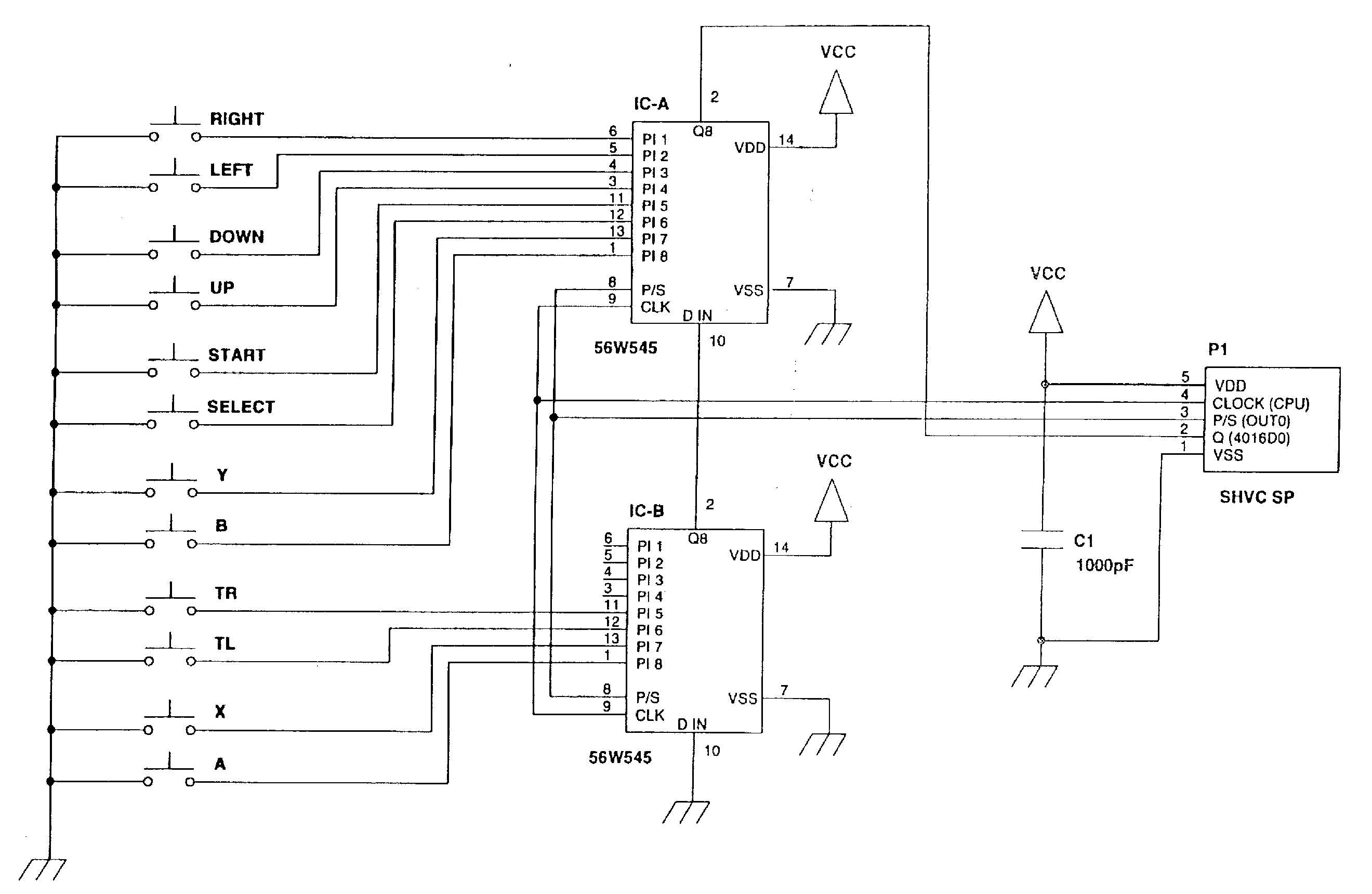
Circuit of the two-IC Super NES controller from Playtronic's Brazilian service manual. Two 56W545 8-bit parallel-in, serial-out shift registers, IC-A and IC-B: IC-A inputs PI1 to PI8 take RIGHT, LEFT, DOWN, UP, START, SELECT, Y and B; IC-B inputs PI5 to PI8 take TR, TL, X and A, and IC-B's Q8 output (pin 2) feeds IC-A's serial input D IN (pin 10). Each button switches its input to ground. VDD is pin 14 and VSS pin 7 on both ICs; P/S is pin 8 and CLK pin 9. The cord connector P1 ("SHVC SP") carries VDD (pin 5), CLOCK (CPU) (pin 4), P/S (OUT0) (pin 3), Q (4016D0) (pin 2) from IC-A's Q8, and VSS (pin 1), with C1, 1000 pF, across the supply.
Source
[edit | edit source]

Cropped from Nintendo / Playtronic, Manual Técnico do Super NES, Rev. 01/94, controller section 4 (PDF page 55), hosted here as File:Manual Tecnico do Super NES Rev 01-94.pdf; described on Nintendo Super NES Technical Manual (Playtronic, Rev. 01-94). Rendered at 300 dpi and converted to greyscale.
Author
[edit | edit source]

Playtronic, for Nintendo.
Licence
[edit | edit source]

Copyright Nintendo and Playtronic. Hosted for preservation and repair reference, with the source cited. Not freely licensed.
File history
Click on a date/time to view the file as it appeared at that time.
| Date/Time | Thumbnail | Dimensions | User | Comment | |
|---|---|---|---|---|---|
| current | 11:09, 25 October 2026 | | 2,640 × 1,720 (37 KB) | Josh (talk | contribs) | Upload for SNES repair guide |
You cannot overwrite this file.
File usage
The following page uses this file:
