

File:Atari 5200 schematic, power supply and power switch latch.png

Summary
[edit | edit source]

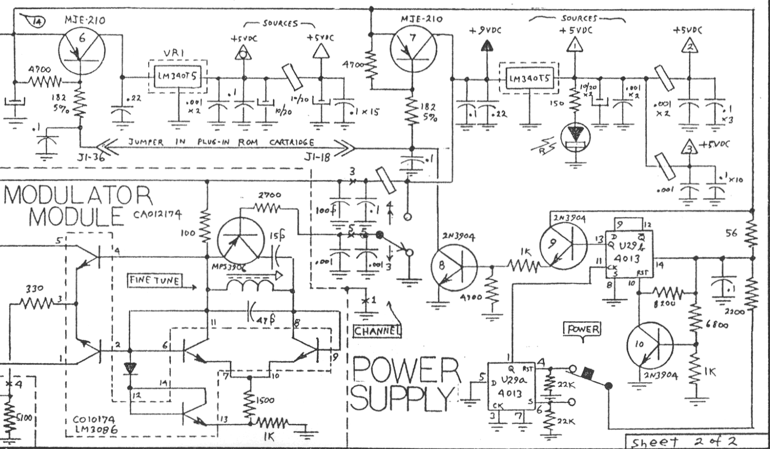
Crop of Atari's 5200 schematic, sheet 2 of 2 (dated 23 February 1983), showing the console power supply: the MJE-210 transistors Q6 and Q7, the LM340T5 regulators VR1 and VR2 with their +5 V sources, the cartridge jumper between J1-36 and J1-18, the power LED and its 150 ohm resistor, the 4013 flip-flop U29 (U29a and U29b), the power switch, and transistors Q8, Q9 and Q10. The RF modulator module occupies the lower left.
Source
[edit | edit source]

Cropped from File:Schematic Atari5200 RFSwitchbox 2000.png, hosted on this wiki.

Author
[edit | edit source]

Atari, Inc.
Licence
[edit | edit source]

Copyright Atari, Inc. Not freely licensed. Hosted for preservation and repair reference, with the source cited.
File history
Click on a date/time to view the file as it appeared at that time.
| Date/Time | Thumbnail | Dimensions | User | Comment | |
|---|---|---|---|---|---|
| current | 11:36, 25 October 2026 | | 1,585 × 925 (322 KB) | Josh (talk | contribs) | Upload for repair guide |
You cannot overwrite this file.
File usage
The following page uses this file:
