

File:Atari 65XE DRAM U9-U16 data bits (Sobola schematic).png

Summary
[edit | edit source]

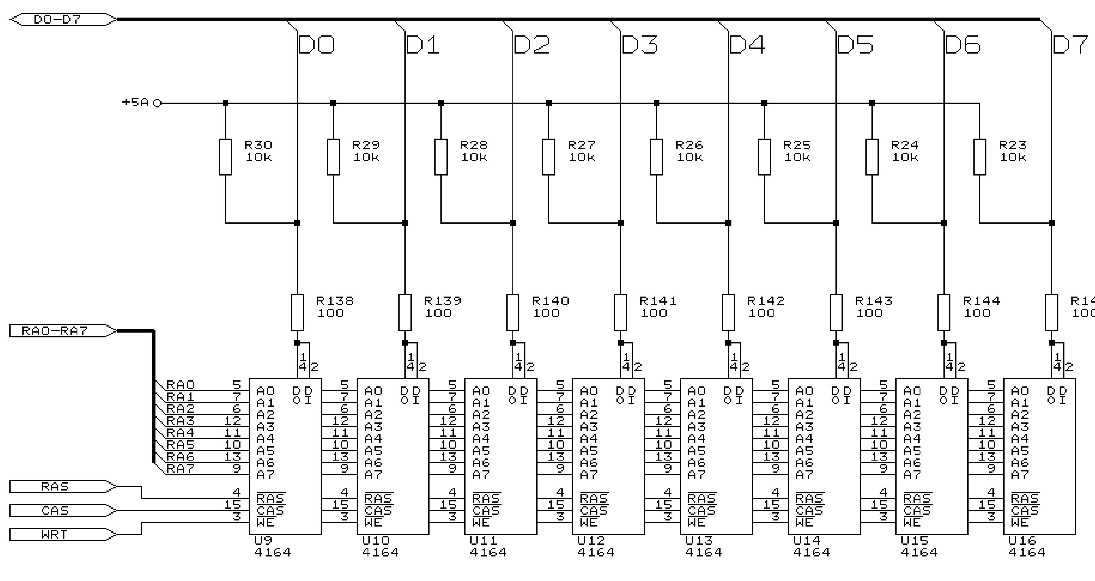
Sheet 4 of Jerzy Sobola's redrawn schematic of the Atari 65XE main board with eight 4164 DRAMs (dated 23 September 2003): U9 to U16, each 64K × 1, on data lines D0 (U9) to D7 (U16). Each data line has a 10 kΩ pull-up to +5A (R30 to R23) and a 100 Ω resistor (R138 to R145) to the chip's data pins 14 and 2. The address lines RA0 to RA7 and the RAS, CAS and write strobes are shared by all eight chips. A community redrawing, not an Atari document.
Source
[edit | edit source]

Cropped from File:ATARI65XE-SCHEMATIC.pdf, sheet 4 of 9, at the file's resolution.
Author
[edit | edit source]

Jerzy Sobola.
Licence
[edit | edit source]

No free licence is stated at the source. Used with credit as a repair reference.
File history
Click on a date/time to view the file as it appeared at that time.
| Date/Time | Thumbnail | Dimensions | User | Comment | |
|---|---|---|---|---|---|
| current | 11:58, 25 October 2026 | | 3,620 × 1,920 (21 KB) | Josh (talk | contribs) | Upload schematic detail for Atari 65XE repair guide |
You cannot overwrite this file.
File usage
The following page uses this file:
