

File:Atari Mega STE clock battery circuit (schematic rev 2 sheet 4).png

Summary
[edit | edit source]

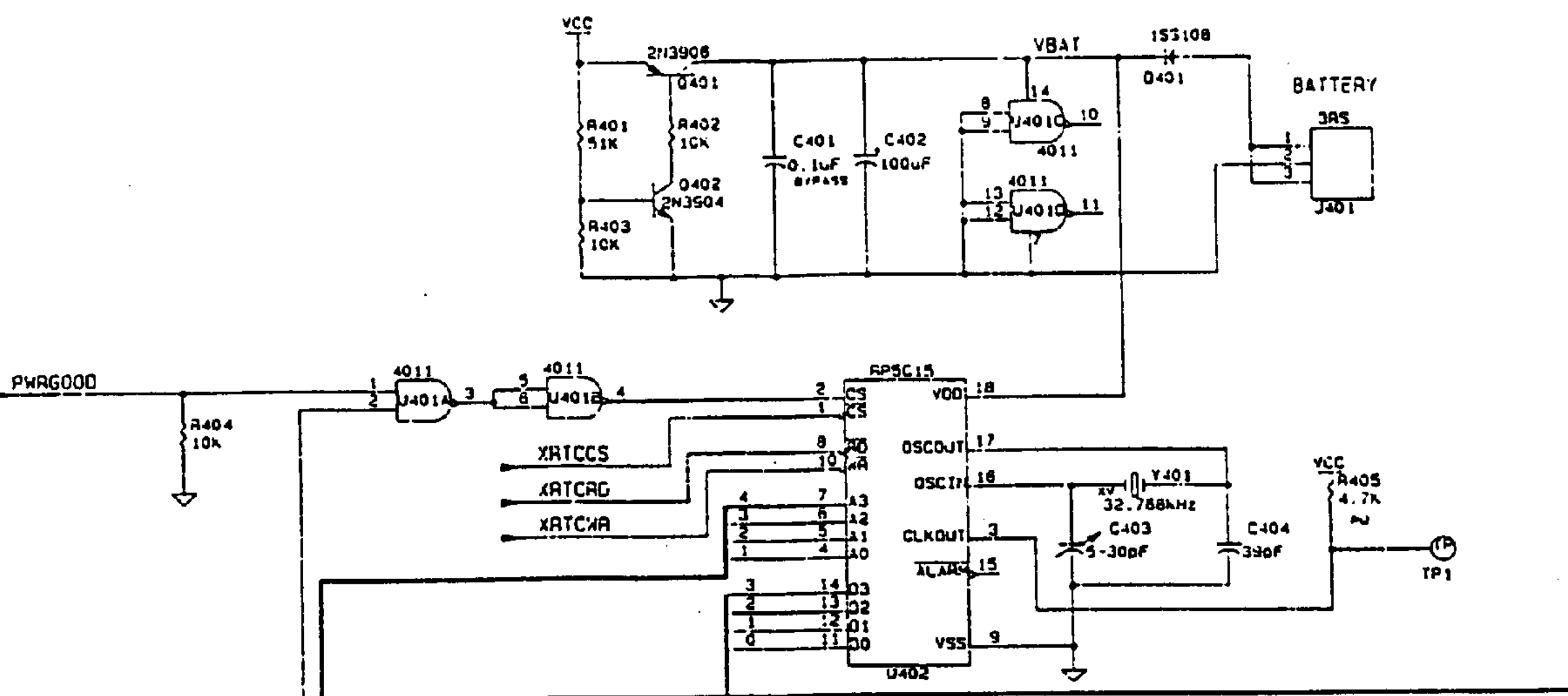
Detail of sheet 4 of Atari's Mega STE main board schematic, revision 2 (April 1990): the Ricoh RP5C15 real-time clock (U402) and its battery supply. The battery plugs into J401, a three-pin connector: pins 1 and 3 are joined and feed the VBAT line through diode D401 (1SS108); pin 2 is ground. With the machine running, VBAT is fed from VCC through Q401 (2N3906), switched by Q402 (2N3904). C401 (0.1 µF) and C402 (100 µF) decouple VBAT, which also supplies the 4011 gates U401 that drive the clock's chip select from PWRGOOD. The crystal Y401 (32.768 kHz) is trimmed by C403 (5–30 pF); CLKOUT (pin 3) goes to test point TP1, pulled up to VCC by R405 (4.7 kΩ).
Source
[edit | edit source]

File:Atari Mega STE Schematic Rev 2.pdf, sheet 4 (PDF page 4), rendered 2026-10-25. See Atari Mega STE Schematic.
Author
[edit | edit source]

Atari Corporation.
Licence
[edit | edit source]

Copyright Atari Corporation. Hosted for preservation and repair reference, with the source cited.
File history
Click on a date/time to view the file as it appeared at that time.
| Date/Time | Thumbnail | Dimensions | User | Comment | |
|---|---|---|---|---|---|
| current | 12:01, 25 October 2026 | | 2,400 × 1,066 (95 KB) | Josh (talk | contribs) | Mega STE clock battery circuit, schematic rev 2 sheet 4 (for Atari Mega STE Clock Battery Replacement) |
You cannot overwrite this file.
File usage
The following page uses this file:
