

File:Atari STE DMA sound circuit (schematic C300780-001 sheet 5).png

Summary
[edit | edit source]

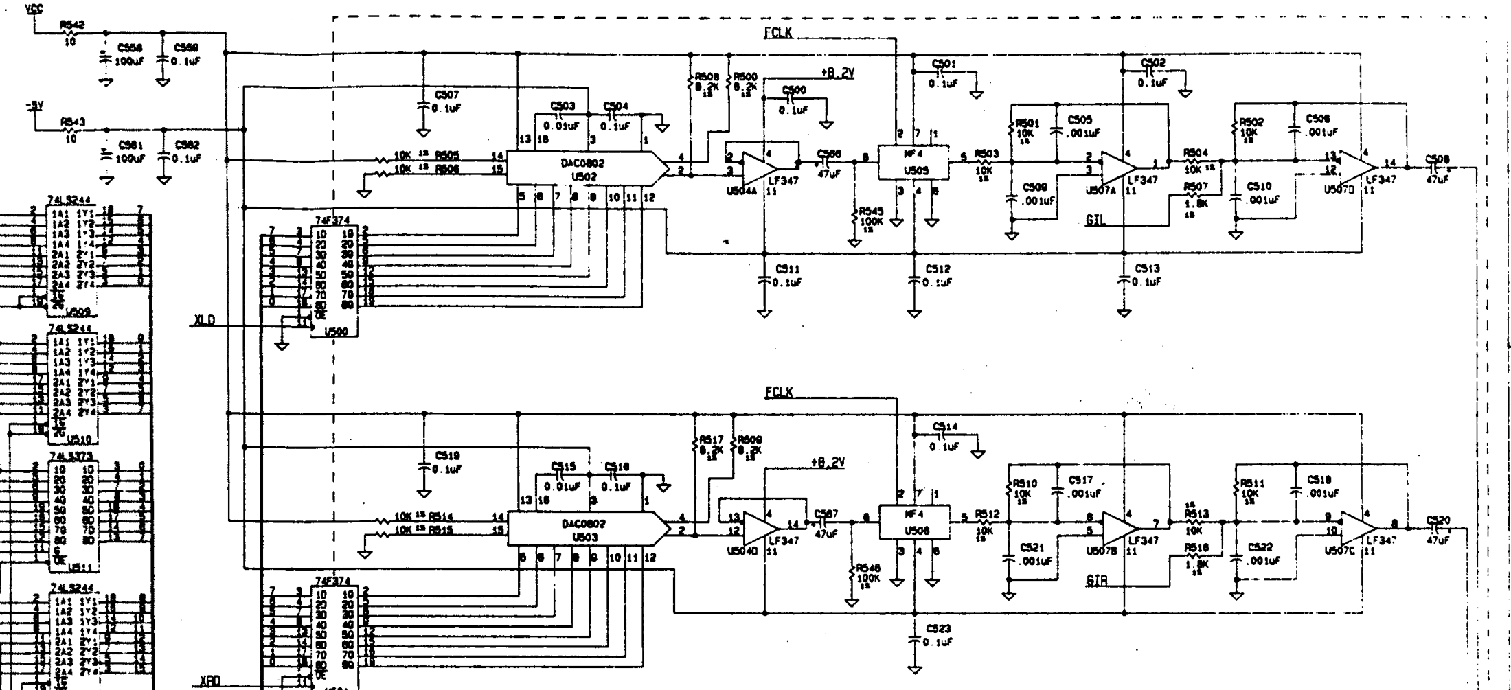
Crop of Atari's STE schematic, drawing C300780-001 revision A (October 1989), sheet 5: the DMA sound channels. For each channel a 74F374 latch (U500 left, loaded by XLD; U501 right, loaded by XRD) feeds a DAC0802 converter (U502, U503), followed by an LF347 buffer, a 47 µF coupling capacitor, an MF4 switched-capacitor filter (U505, U506, clocked by FCLK) and two more LF347 stages, to the GIL and GIR outputs. The converter supplies come from VCC through R542 (10 Ω, with C556, 100 µF) and from −5 V through R543 (10 Ω, with C561, 100 µF); the op-amps run from +8.2 V. Cropped from File:Atari STE Schematic Rev A C300780-001.pdf.
Source
[edit | edit source]

File:Atari STE Schematic Rev A C300780-001.pdf (rendered 2026-10-25).
Author
[edit | edit source]

Atari Corporation.
Licence
[edit | edit source]

Copyright Atari Corporation. Hosted for preservation and repair reference, with the source cited.
File history
Click on a date/time to view the file as it appeared at that time.
| Date/Time | Thumbnail | Dimensions | User | Comment | |
|---|---|---|---|---|---|
| current | 11:40, 25 October 2026 | | 2,200 × 1,005 (239 KB) | Josh (talk | contribs) | Crop of Atari STE schematic for DMA sound repair guide |
You cannot overwrite this file.
File usage
The following page uses this file:
