

File:Casio PV-7 main board.jpg
Summary
[edit | edit source]

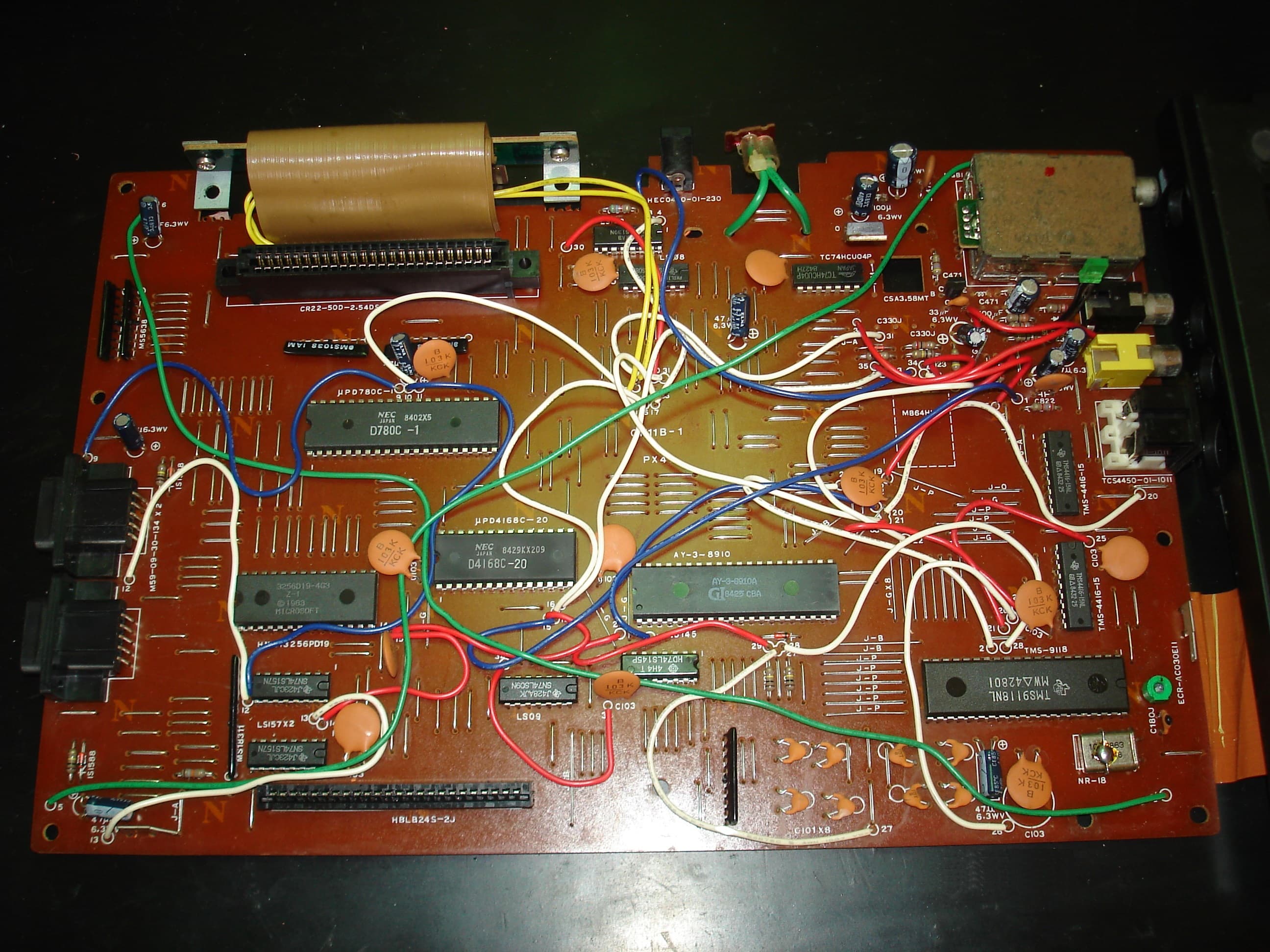
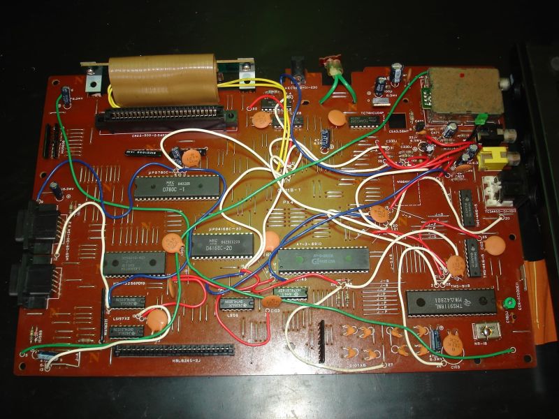
Main board of a Casio PV-7, component side, with many factory jumper wires. Visible: cartridge connector CR22-50D at the top, NEC D780C-1 CPU, Microsoft 32 KB BASIC ROM, NEC D4168C-20 RAM, TMS9118NL video chip with two TMS4416 video RAMs, AY-3-8910A sound chip, the silkscreen marking for the Fujitsu MB64H131 (the chip itself is on the solder side), RF modulator, the DC input socket and power switch at the top edge, the two joystick connectors at the left and the KB-7 expansion connector HBLB24S-2J at the bottom edge.
Source
[edit | edit source]

MSX Resource Center wiki, file page https://www.msx.org/wiki/File:Pv7b.jpg, current version uploaded by Mars2000you on 8 February 2016 with the description "Casio PV-7 PCB". Retrieved 2026-10-21.

Author
[edit | edit source]

Photograph uploaded to the MSX Resource Center wiki by Mars2000you; the original photographer is not named there.
Licence
[edit | edit source]

No licence is stated on the source page; copyright remains with the photographer. Hosted for repair reference, with the source cited.
File history
Click on a date/time to view the file as it appeared at that time.
| Date/Time | Thumbnail | Dimensions | User | Comment | |
|---|---|---|---|---|---|
| current | 14:44, 21 October 2026 | | 2,592 × 1,944 (515 KB) | Josh (talk | contribs) | Upload for the Casio PV-7 and PV-16 pages |
You cannot overwrite this file.
File usage
The following 3 pages use this file:
