

File:Jumper wire routing and bonding (diagram).png

Summary
[edit | edit source]

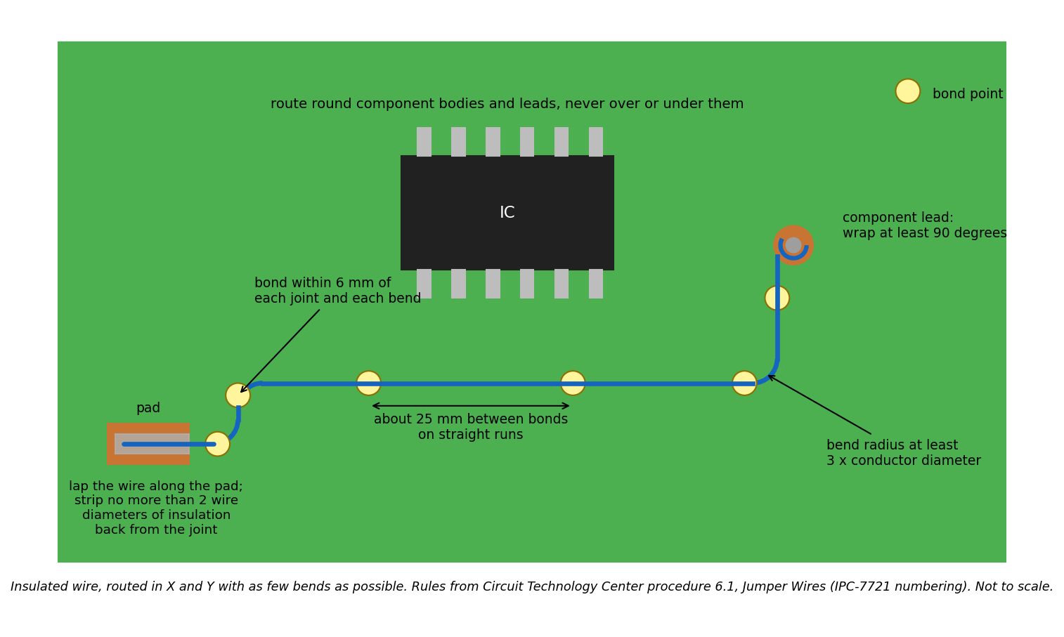
Plan-view diagram of a jumper wire added to a circuit board. The insulated wire is lapped along a pad at one end and wrapped at least 90 degrees round a component lead at the other, routed in X and Y with few bends and round the IC body, and bonded to the board within 6 mm of each joint and each bend and at about 25 mm intervals on straight runs. Bends are no tighter than three times the conductor diameter, and insulation is stripped back no more than two wire diameters from a joint. Not to scale.
Source
[edit | edit source]

Drawn for this wiki (2026-10-25). The rules are from Circuit Technology Center, procedure 6.1, Jumper Wires.
Author
[edit | edit source]

RetroTechCollection wiki.
Licence
[edit | edit source]

Drawn for this wiki and released under Creative Commons Attribution-ShareAlike 4.0.
File history
Click on a date/time to view the file as it appeared at that time.
| Date/Time | Thumbnail | Dimensions | User | Comment | |
|---|---|---|---|---|---|
| current | 14:49, 25 October 2026 | | 1,514 × 907 (106 KB) | Josh (talk | contribs) | Upload for the PCB repair technique pages |
You cannot overwrite this file.
File usage
The following page uses this file:
