

File:Philips Odyssey 2100 schematic (CS43618).jpg
Summary
[edit | edit source]

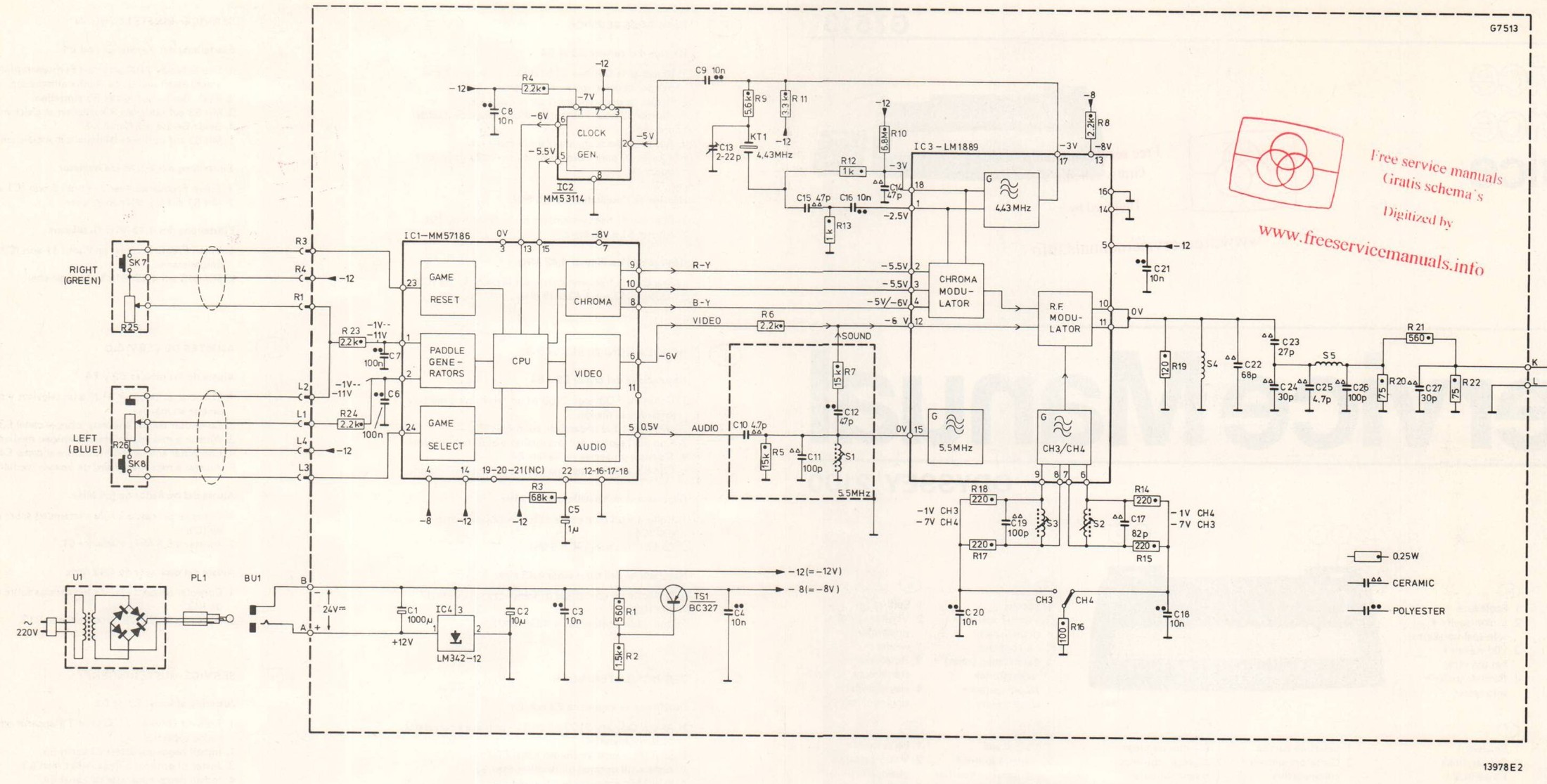
The schematic of the Philips Odyssey 2100 (type G7513), drawing 13978E2, from page 3 of the Philips service manual CS43618: the adaptor U1, the LM342-12 regulator IC4 and the BC327 TS1, the game chip IC1 (MM57186), the clock generator IC2 (MM53114), the LM1889 modulator IC3 with the 4.43 MHz crystal KT1, the 5.5 MHz sound tank S1 and the channel E3/E4 coils S3 and S2, and the two controllers with their potentiometers R25 and R26 and buttons SK7 and SK8. DC voltages are marked at most IC pins. Rendered from File:Philips Odyssey 2100 Service Manual CS43618.pdf and reduced to 2200 pixels wide. The red stamp is the scanner's.
Source
[edit | edit source]

Internet Archive item MagnavoxOdyssey, file "Philips Odyssey 2100 (model G7513) Service Manual.pdf" (retrieved 2026-10-20). The item description credits the scan to Wil Manshande of www.freeservicemanuals.info; each page carries that site's stamp.
Author
[edit | edit source]

Philips (service documentation).
Licence
[edit | edit source]

Copyright Philips. Hosted for preservation and repair reference, with the source cited.
File history
Click on a date/time to view the file as it appeared at that time.
| Date/Time | Thumbnail | Dimensions | User | Comment | |
|---|---|---|---|---|---|
| current | 23:47, 20 October 2026 | | 2,200 × 1,116 (355 KB) | Josh (talk | contribs) | Schematic from Philips service manual CS43618 |
You cannot overwrite this file.
File usage
The following 2 pages use this file:
