

File:SGI R8000 CPU module component layout (108-0130-001 Figure 1-2).png

Summary
[edit | edit source]

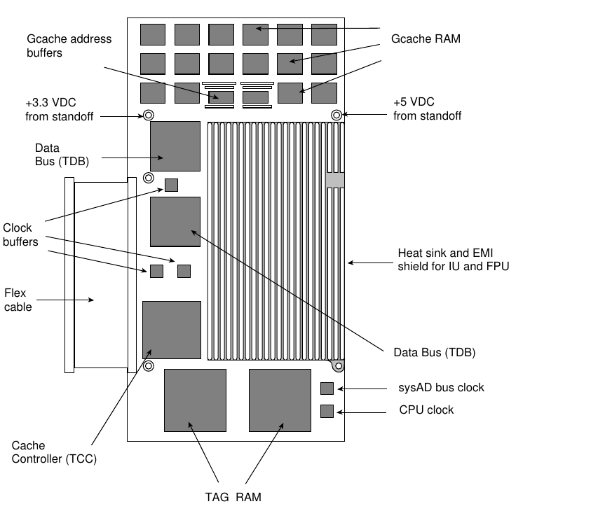
Figure 1-2, "R8000 CPU Board Component Layout", from Silicon Graphics' POWER Indigo2 and POWER CHALLENGE M Upgrade Instructions (108-0130-001, 1994), page 1-4. Line drawing of the R8000 CPU module used in the POWER Indigo² and POWER CHALLENGE M: the heat sink and EMI shield over the integer and floating-point chips, the global cache RAM and address buffers, the TDB data bus chips, the cache controller (TCC), the two tag RAMs, the clock buffers and clocks, the flex cable, and the +3.3 V and +5 V feeds through the standoffs. Rendered from the PDF at 150 dpi and cropped to the figure. See SGI Power Indigo².
Source
[edit | edit source]

File:SGI POWER Indigo2 and POWER CHALLENGE M Upgrade Instructions (108-0130-001).pdf, page 1-4 (PDF page 12). That PDF came from the Jurassic.nl TechPubs archive.
Author
[edit | edit source]

Silicon Graphics, Inc. (illustrated by Dany Galgani, as credited in the document)
Licence
[edit | edit source]

Copyright 1994 Silicon Graphics, Inc. Hosted for preservation and repair reference, with the source cited.
File history
Click on a date/time to view the file as it appeared at that time.
| Date/Time | Thumbnail | Dimensions | User | Comment | |
|---|---|---|---|---|---|
| current | 00:31, 22 October 2026 | | 853 × 750 (54 KB) | Josh (talk | contribs) | Figure 1-2 from SGI 108-0130-001 |
You cannot overwrite this file.
File usage
The following 2 pages use this file:
