

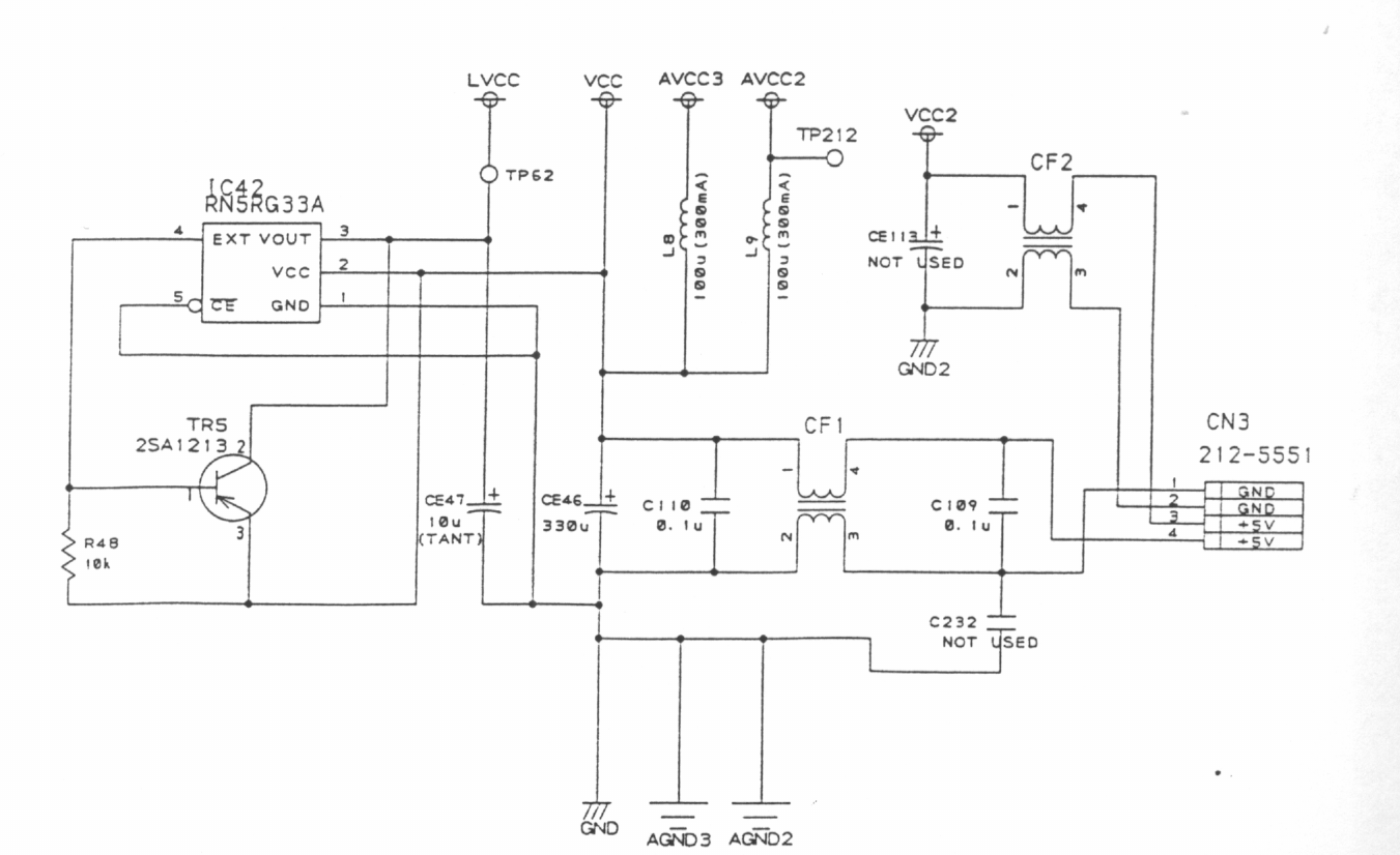
File:Sega Saturn VA13 power input and 3.3 V regulator schematic.png

Summary
[edit | edit source]

The power input section of the Saturn VA13 main board schematic (main schematic diagram sheet 10/11): connector CN3 (212-5551) with two ground and two +5 V pins, the common-mode chokes CF1 and CF2, CE46, the 3.3 V LVCC regulator IC42 (RN5RG33A) with pass transistor TR5 (2SA1213), CE47 and test point TP62, and the chokes L8 and L9 to AVCC3 and AVCC2.
Source
[edit | edit source]

Conjunto P.C.I. VA-13, a schematic set for the Sega Saturn VA13 main board with Portuguese title blocks, scanned by Brasilmodchip (www.brasilmodchip.com.br), PDF page 11, cropped. Hosted on this wiki as File:Sega Saturn VA13 Service Manual PAL.pdf; see Sega Saturn VA13 Service Manual (PAL).
Author
[edit | edit source]

Not stated on the drawing; the circuit is Sega's. Scanned by Brasilmodchip.
Licence
[edit | edit source]

Copyright of the original drawing's owner. Hosted for preservation and repair reference, with the source cited.
File history
Click on a date/time to view the file as it appeared at that time.
| Date/Time | Thumbnail | Dimensions | User | Comment | |
|---|---|---|---|---|---|
| current | 11:04, 25 October 2026 | | 1,351 × 826 (237 KB) | Josh (talk | contribs) | Upload for repair guide |
You cannot overwrite this file.
File usage
The following page uses this file:
