

File:Sharp X68030 main board component side (X68030 Inside Out).jpg

Summary
[edit | edit source]

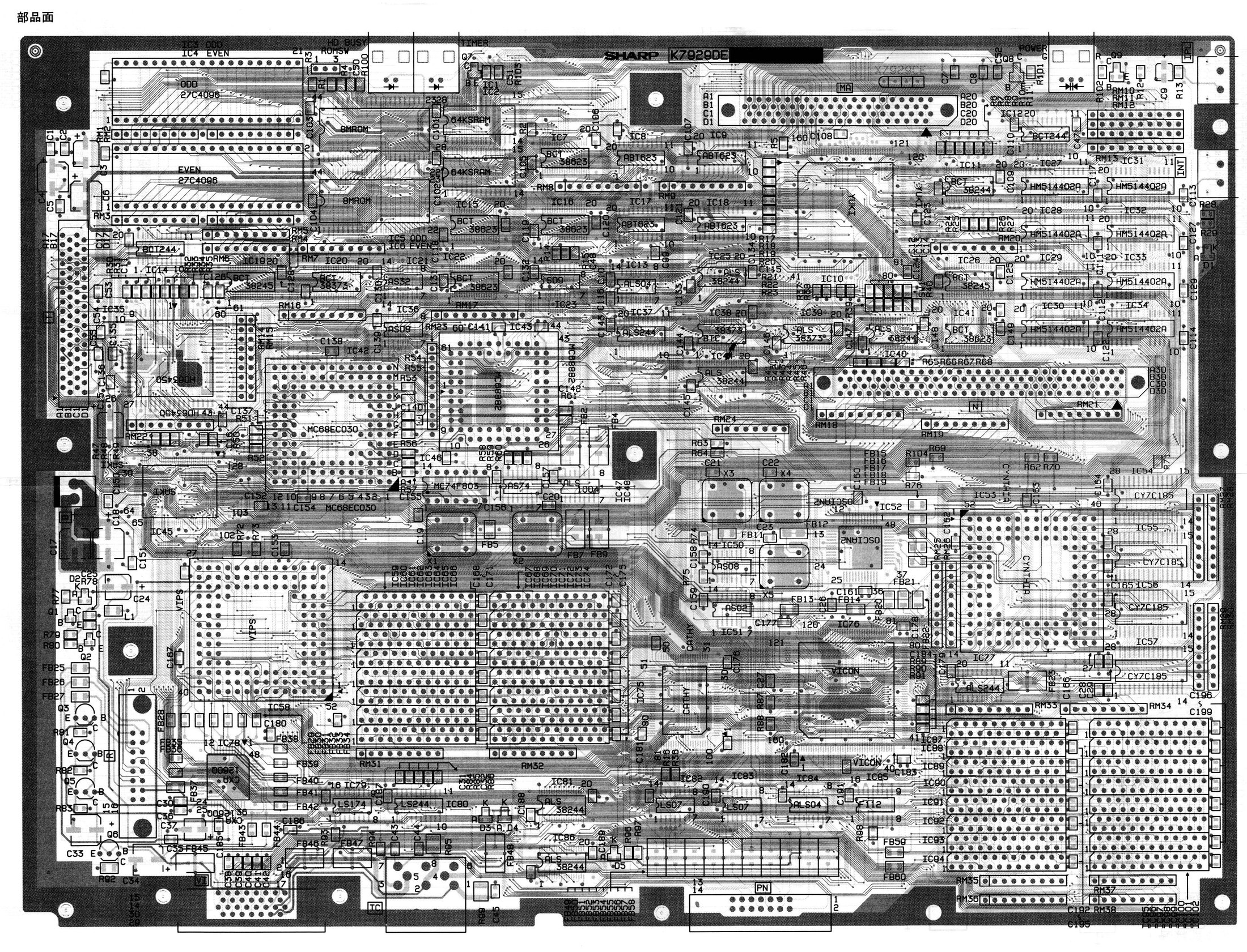
Sharp's layout drawing of the component side (部品面) of the X68030 main board, marked K7929DE (unit DUNTK7929DE01, bare board QPWBX7929CEZZ on the schematic). The drawing shows the MC68EC030 and MC68882 sockets, the custom chips VIPS, CYNTHIA, VICON, CATHY, OSCIAN2, YUKI and SAKI, the eight HM514402A DRAMs, the IPL ROMs IC3 and IC4 (27C4096), the 8 Mbit character ROMs, and the positions of the electrolytic capacitors. This image is page 9 of the schematic set, cropped to the board and reduced to 2200 pixels wide. The full-resolution page is in File:Sharp X68030 Schematic (X68030 Inside Out, 1994).pdf.
Source
[edit | edit source]

Scanned from the schematic appendix of 桑野雅彦 (Kuwano Masahiko), X68030 Inside/Out, SoftBank, 30 March 1994. Internet Archive item X68030InsideOut1994, file X68030_schematic.pdf: https://archive.org/details/X68030InsideOut1994 (retrieved 2026-10-21).
Author
[edit | edit source]

Sharp Corporation (board drawing), as reproduced in Kuwano Masahiko's book; scan uploaded to the Internet Archive by its contributor.
Licence
[edit | edit source]

Copyright Sharp Corporation and SoftBank. Not freely licensed. Hosted for preservation and repair reference.
File history
Click on a date/time to view the file as it appeared at that time.
| Date/Time | Thumbnail | Dimensions | User | Comment | |
|---|---|---|---|---|---|
| current | 18:12, 21 October 2026 | | 2,200 × 1,681 (1.6 MB) | Josh (talk | contribs) | X68030 main board K7929DE component-side layout, page 9 of the X68030 Inside/Out schematic set |
You cannot overwrite this file.
File usage
The following 2 pages use this file:
