

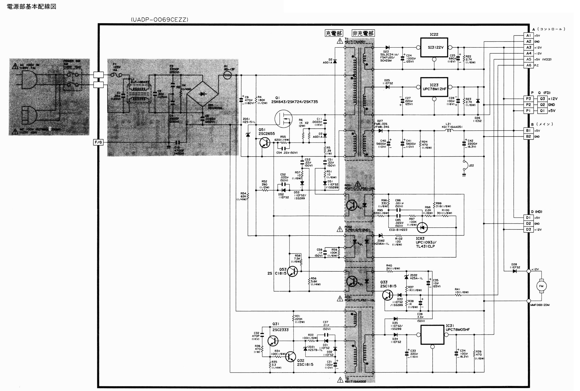
File:Sharp X68030 power supply schematic (X68030 Inside Out).jpg

Summary
[edit | edit source]

Sharp's power supply schematic (電源部基本配線図, "power supply basic wiring diagram") for the X68030 (CZ-500C/CZ-510C). The board is UADP-0069CEZZ, the unit owners call the SH4. The drawing shows the 100 V input, fuse F1 (125 V 4 A), bridge DB1, reservoir C9 (470 µF 180 V), switching MOSFET Q1, transformer T1 with the +12 V (IC22 SI3122V), −12 V (IC23 µPC78M12HF) and +5 V outputs, the standby converter round T2 with IC31 (µPC78M05HF) for the +5 V VCC2 rail, the fan, and output connectors A (control board), B (main board), P/Q (floppy drives) and D (hard disk). This image is page 19 of the schematic set, cropped to the drawing and reduced to 2200 pixels wide. The full-resolution page is in File:Sharp X68030 Schematic (X68030 Inside Out, 1994).pdf.
Source
[edit | edit source]

Scanned from the schematic appendix of 桑野雅彦 (Kuwano Masahiko), X68030 Inside/Out, SoftBank, 30 March 1994. Internet Archive item X68030InsideOut1994, file X68030_schematic.pdf: https://archive.org/details/X68030InsideOut1994 (retrieved 2026-10-21).
Author
[edit | edit source]

Sharp Corporation (circuit diagram), as reproduced in Kuwano Masahiko's book; scan uploaded to the Internet Archive by its contributor.
Licence
[edit | edit source]

Copyright Sharp Corporation and SoftBank. Not freely licensed. Hosted for preservation and repair reference.
File history
Click on a date/time to view the file as it appeared at that time.
| Date/Time | Thumbnail | Dimensions | User | Comment | |
|---|---|---|---|---|---|
| current | 18:12, 21 October 2026 | | 2,200 × 1,486 (535 KB) | Josh (talk | contribs) | X68030 power supply schematic, page 19 of the X68030 Inside/Out schematic set |
You cannot overwrite this file.
File usage
The following 2 pages use this file:
