

File:Sinclair QL circuit diagram (Issue 6), RAM data pins.png
Size of this preview: 465 × 600 pixels. Other resolution: 620 × 800 pixels.

Original file (620 × 800 pixels, file size: 13 KB, MIME type: image/png)
Summary
[edit | edit source]

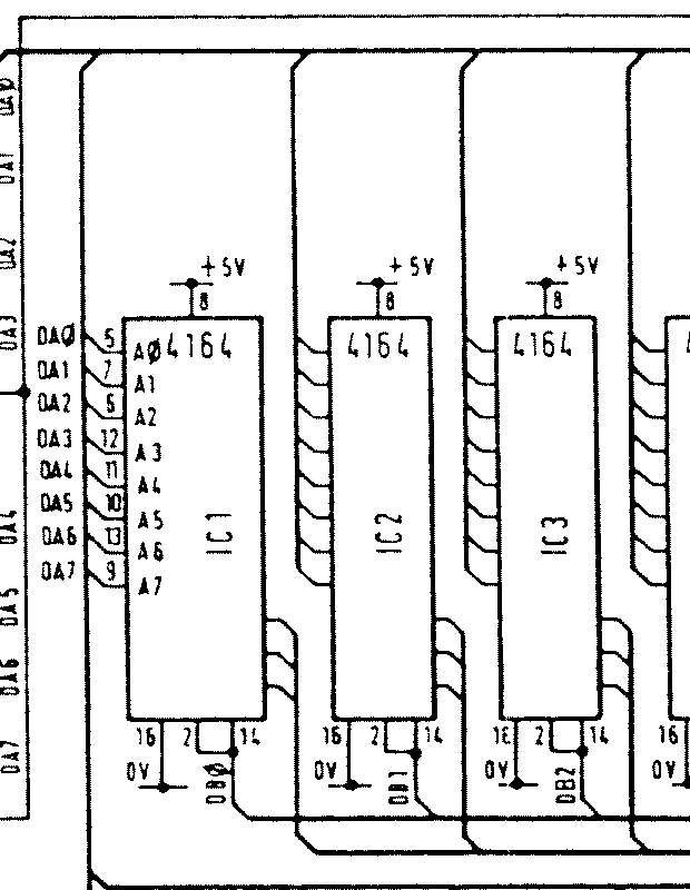
Part of Sinclair's Issue 6 circuit diagram for the Sinclair QL: RAM chips IC1, IC2 and IC3 (type 4164), with address lines DA0 to DA7 on pins 5, 7, 6, 12, 11, 10, 13 and 9, +5 V on pin 8, 0 V on pin 16, and pins 2 and 14 joined to data lines DB0, DB1 and DB2.
Source
[edit | edit source]

Cropped from File:Sinclair QL circuit diagram (Issue 6).png, Sinclair's Issue 6 circuit diagram (QL Service Manual, Figure 1.5, page 1.18).

Author
[edit | edit source]

Sinclair Research Ltd
Licence
[edit | edit source]

Copyright Sinclair Research Ltd. Reproduced from the service manual for repair reference; not freely licensed.
File history
Click on a date/time to view the file as it appeared at that time.
| Date/Time | Thumbnail | Dimensions | User | Comment | |
|---|---|---|---|---|---|
| current | 11:18, 25 October 2026 | | 620 × 800 (13 KB) | Josh (talk | contribs) | Upload for repair guide |
You cannot overwrite this file.
File usage
The following page uses this file:
