

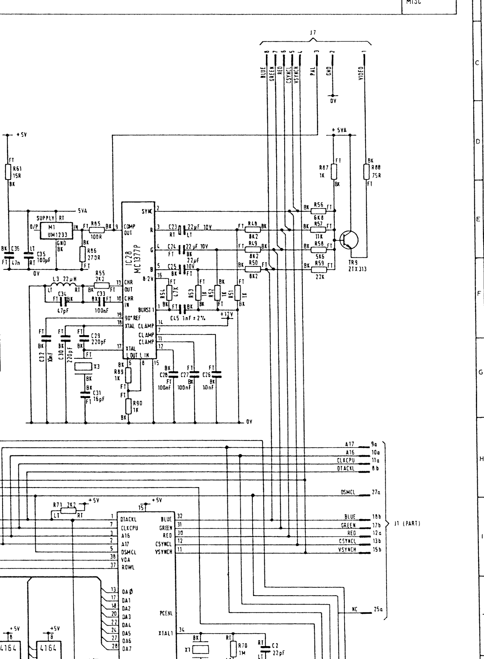
File:Sinclair QL video output circuit (Issue 6).png

Summary
[edit | edit source]

The same video output section on the Issue 6 circuit diagram: J7, IC28 and its resistors, TR9 with R56 to R59, R87 and R88, M1, and the five video outputs of the ZX8301 (IC22) running to J7 and J1. The connections and designators match the Issue 5 diagram. The J7 pin numbers printed here are the mirror image of the numbering in the QL User Guide and the Service Manual's Appendix A. Cropped from Figure 1.5 of Sinclair's QL Service Manual (issue 3, October 1985), page 1.18 (PDF page 20) of the hosted copy File:Sinclair QL Service Manual.pdf. Used on Sinclair QL RGB Port Repair.
Source
[edit | edit source]

Cropped for this wiki from File:Sinclair QL circuit diagram (Issue 6).png, the wiki's copy of Figure 1.5; no other change.

Author
[edit | edit source]

Sinclair Research Ltd
Licence
[edit | edit source]

Copyright Sinclair Research Ltd. Not freely licensed. Hosted for preservation and repair reference, with the source cited.
File history
Click on a date/time to view the file as it appeared at that time.
| Date/Time | Thumbnail | Dimensions | User | Comment | |
|---|---|---|---|---|---|
| current | 10:42, 25 October 2026 | | 1,616 × 2,200 (424 KB) | Josh (talk | contribs) | Crop for Sinclair QL RGB Port Repair |
You cannot overwrite this file.
File usage
The following page uses this file:
