

File:Super Famicom power circuit (Nintendo service manual).png

Summary
[edit | edit source]

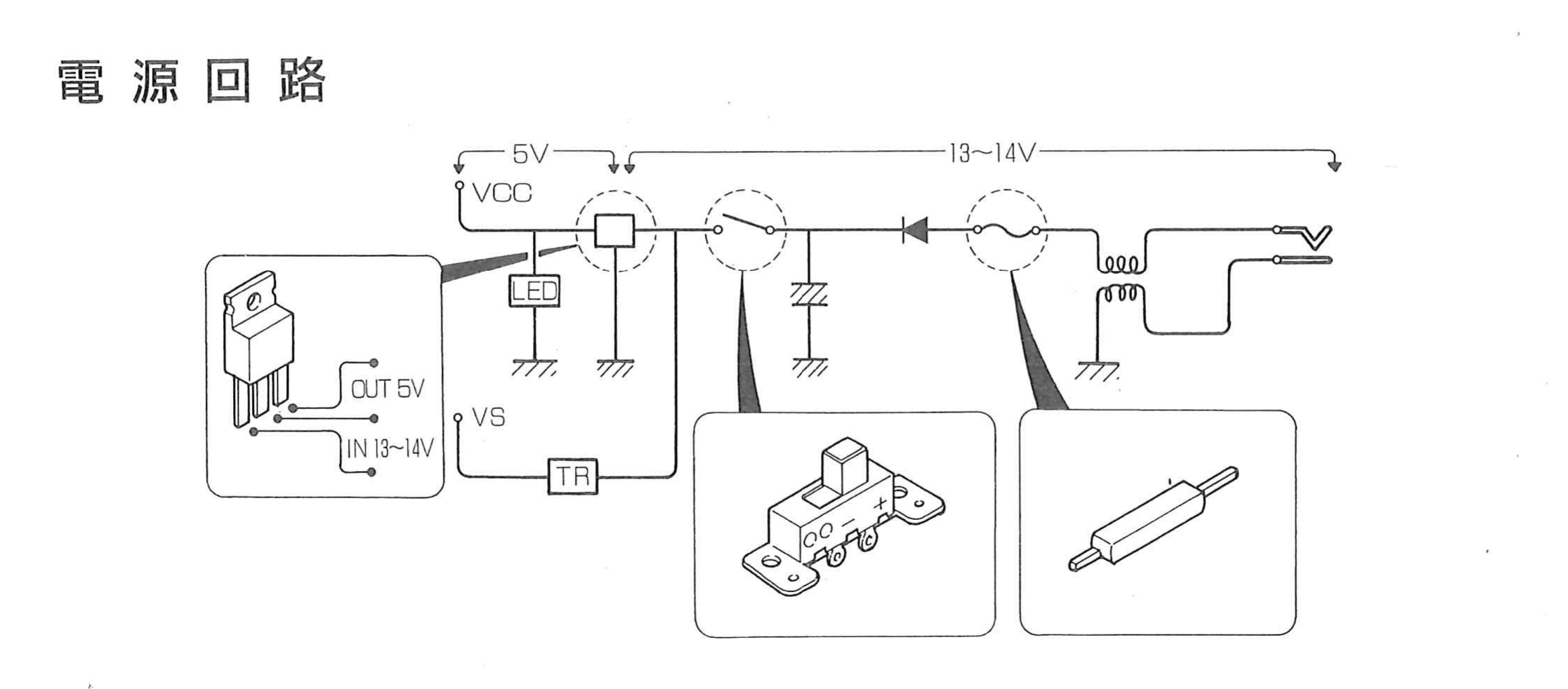
Nintendo's power-circuit diagram for the Super Famicom (SHVC), titled 電源回路 (power circuit). From right to left: the DC input, a line filter, the fuse (drawn as an axial part in the inset), a series diode, a capacitor, the power switch (drawn in the inset with its + and − markings), the 7805 regulator (inset: IN 13-14 V, OUT 5 V) feeding VCC and the power LED, and a transistor (TR) feeding the VS rail. The span from the input to the regulator is marked 13-14 V and the regulator output 5 V.
Source
[edit | edit source]

Cropped from Nintendo's ファミコン・スーパーファミコン・ゲームボーイ サービスマニュアル (Famicom / Super Famicom / Game Boy Service Manual), 1992, printed page 12 (PDF page 7), hosted here as File:Nintendo Famicom Service Manual.pdf; described on Nintendo Famicom Service Manual. Rendered at 300 dpi and converted to greyscale.
Author
[edit | edit source]

Nintendo Co., Ltd.
Licence
[edit | edit source]

Copyright Nintendo Co., Ltd. Hosted for preservation and repair reference, with the source cited. Not freely licensed.
File history
Click on a date/time to view the file as it appeared at that time.
| Date/Time | Thumbnail | Dimensions | User | Comment | |
|---|---|---|---|---|---|
| current | 10:46, 25 October 2026 | | 2,233 × 982 (183 KB) | Josh (talk | contribs) | Upload for SNES repair guide |
You cannot overwrite this file.
File usage
The following page uses this file:
