
File:Atari 400 motherboard and power supply board (Knurrikowski).png

Summary
[edit | edit source]

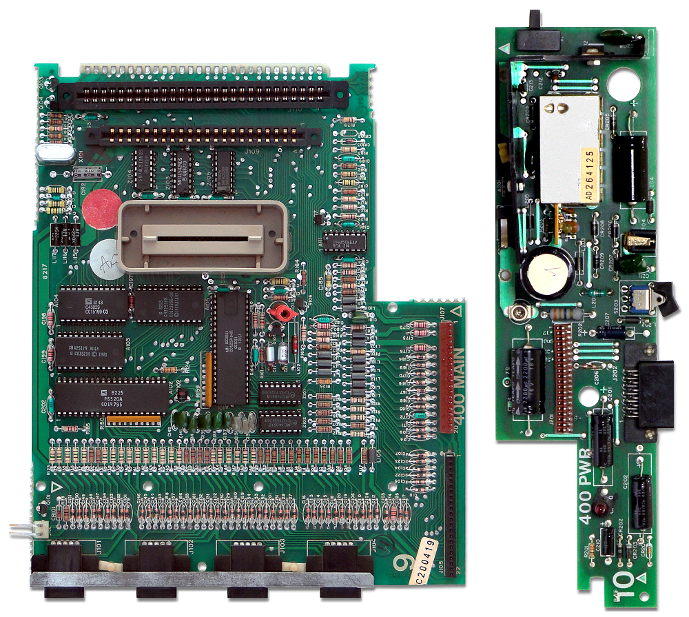
An Atari 400 motherboard (left, silkscreen "400 MAIN") and power supply board (right, silkscreen "400 PWR"). On the motherboard: the four controller jacks J101 to J104 along the bottom edge, the cartridge socket in the centre, the CPU and RAM card connectors J110 and J109 at the top, the operating system ROMs A103, A104 and A105 and the PIA (A102) at the left, POKEY (A101) in the centre, the keyboard multiplexers Z101 and Z102 to its right, the crystal X101 at top left and the keyboard connector J105 at the lower right. On the power supply board: the RF modulator can, the regulators and electrolytic capacitors, the 13-pin peripheral socket J202 and the power switch.
Source
[edit | edit source]

Atari 400 mainboard and daughterboard.png on Wikimedia Commons (retrieved 2026-10-25).

Author
[edit | edit source]

Knurrikowski (Wikimedia Commons).
Licence
[edit | edit source]

File history
Click on a date/time to view the file as it appeared at that time.
| Date/Time | Thumbnail | Dimensions | User | Comment | |
|---|---|---|---|---|---|
| current | 20:00, 25 October 2026 | | 1,000 × 895 (1.62 MB) | Josh (talk | contribs) | From Wikimedia Commons |
You cannot overwrite this file.
File usage
The following file is a duplicate of this file (more details):

- File:Atari 400 mainboard and daughterboard.png from Wikimedia Commons
The following 2 pages use this file:
