
IBM PC (5150) RAM Replacement

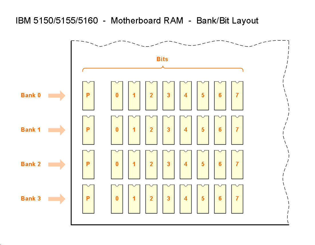
The IBM PC (5150) system board carries its RAM in four banks of nine dynamic RAM chips: eight chips for the data bits and one for parity in each bank.[1] Bank 0 is soldered to the board and banks 1 to 3 are in sockets on both versions of the board.[2][3][4] The 16KB-64KB board uses 4116 chips (16K by 1 bit) and the 64KB-256KB board uses 4164 chips (64K by 1 bit).[2][3] Minuszerodegrees.net describes vintage RAM chips as having a relatively high failure rate.[5]
The repair starts from the power-on self test (POST) error, finds the failed chip and replaces it. A chip in banks 1 to 3 is changed with IBM's own removal and replacement procedure. A chip in bank 0 has to be found by other means and desoldered.
Symptoms
[edit | edit source]- An error of the form aabb 201 at power-on, for example 0510 201. aa is the 4 KB block that holds the fault and bb is the failing bit. After a 201 the screen may clear and show PARITY CHECK 1.[2][3]
- A board that appears dead, with no picture and no beep. The POST tests the first 16 KB before anything else and halts silently if it finds a fault there, so a failed chip in bank 0 looks like a dead board.[5] The dead-board symptom has many other causes; work through the troubleshooting guide's checks for a machine with no beep and no picture first.
- On the 64KB-256KB board, the first 16 KB is only the first quarter of each bank 0 chip. A bank 0 chip that fails only in its upper three quarters gives a 201 error instead of a dead board; a fault at 32 KB, for example, gives a block of 08.[3]
Errors that look like a RAM fault but are not a single failed chip:
- A bb value other than 00, 01, 02, 04, 08, 10, 20, 40 or 80 means several bits at once. Often the POST is testing RAM that is not there: SW1 and SW2 set for more memory than is fitted, or a memory card that is faulty or set up wrongly. Removing the memory card from minuszerodegrees' 64KB-256KB machine without changing the switches gave 4098 201.[3][2]
- With the 10/27/82 BIOS, the POST miscalculates the memory unless all four system board banks are filled and the switches set to match. On a 16KB-64KB board upgraded to that BIOS this almost always gives a 201 error such as 1094 201.[2][6]
- A block of 10 or higher on the 16KB-64KB board, or 40 or higher on the 64KB-256KB board, is RAM on an expansion card, not on the system board.[2][3][7]
Safety
[edit | edit source]Switch the system unit off, unplug the power cord and disconnect every cable from the rear before removing anything.[8] RAM chips can be damaged by electrostatic discharge from your body.[9]
Tools and parts
[edit | edit source]- An IC extractor. IBM's service manual lists a tweezer-type module puller as a special tool for removing memory.[10]
- A multimeter, for checking the supply pins on a 16KB-64KB board.[5]
- For bank 0: desoldering tools, and a diagnostic ROM for socket U33 (see below).[5]
- Replacement chips. The access time in IBM's Technical Reference is 250 ns, and faster parts work.[2][3][4]
| Board marking | Chip type | Access time | Banks and addresses | Notes |
|---|---|---|---|---|
| 16KB-64KB CPU | 4116 (16K × 1) | 250 ns or faster (for example 200 ns) | Bank 0: 0000 to 3FFF hex Bank 1: 4000 to 7FFF Bank 2: 8000 to BFFF Bank 3: C000 to FFFF |
Needs +12 V, +5 V and −5 V. Do not fit a "+5 V only" 16K chip. |
| 64KB-256KB CPU | 4164 (64K × 1) | 250 ns or faster | Bank 0: 00000 to 0FFFF hex Bank 1: 10000 to 1FFFF Bank 2: 20000 to 2FFFF Bank 3: 30000 to 3FFFF |
Use the type with pin 1 not connected. |
Sources: minuszerodegrees.net RAM pages for each board.[2][3]

The 4116 is powered from three rails: −5 V on pin 1, +12 V on pin 8 and +5 V on pin 9, with ground on pin 16. Some makers produced "+5 V only" 16K chips that moved +5 V from pin 9 to pin 8. Fitted in a 4116 socket, such a chip gets +12 V on its +5 V pin and is likely to be damaged. Minuszerodegrees gives the Mostek MK4516, Intel 2118, Hitachi HM4816 and Fujitsu MB8118 as examples.[11] Not every chip sold as a 4116 has "4116" in its part number; minuszerodegrees lists equivalents by maker, with access times.[12] On the 4164, pin 1 is unused on most types, but on some it selects extra refresh modes.[13]
IBM's parts catalogue for the first system board lists part 8529142, "16KB Memory Module".[14]
Procedure
[edit | edit source]Identify the board
[edit | edit source]- Find the marking printed on the system board: "16KB-64KB CPU" or "64KB-256KB CPU". The RAM type, the error decoding and the bank 0 test all depend on it.[2][3]

Decode the error
[edit | edit source]
- Write down the four characters in front of 201. The first two (aa) are the block and the last two (bb) the bit.[2][7]
- Find the bank from aa in the table below.[2][3]
- Find the chip from bb: 00 is the parity chip, and 01, 02, 04, 08, 10, 20, 40 and 80 are data bits 0 to 7.[2][7] IBM's example 0C40 201 is bank 3, bit 6 on the 16KB-64KB board, and its example 3040 201 is bank 3, bit 6 on the 64KB-256KB board.[15]
- If bb is not one of those nine values, convert it to binary: each 1 is a failing bit. The value 4C, for example, is bits 6, 3 and 2.[16] Check the switches and any memory card before suspecting several chips.[3]
| Bank | 16KB-64KB board | 64KB-256KB board |
|---|---|---|
| Bank 0 (soldered) | 00 to 03 (never shown: the POST halts instead) | 00 to 0F (00 to 03 halts the POST) |
| Bank 1 | 04 to 07 | 10 to 1F |
| Bank 2 | 08 to 0B | 20 to 2F |
| Bank 3 | 0C to 0F | 30 to 3F |
| Expansion card RAM | 10 to 9F | 40 to 9F |
Sources: minuszerodegrees.net;[2][3] IBM's 1981 chart gives the 16KB-64KB bank codes as 00, 04, 08 and 0C.[7]
Find the chip on the board
[edit | edit source]
- Turn the board so that the rear panel is at the top, as in IBM's drawings. Each bank is then a row of nine chips with the parity chip on the left and bits 0 to 7 to its right, bank 0 nearest the rear.[1][7][8]
- On the board itself, the silkscreen marks BANK 0 to BANK 3 and BIT P, BIT 0 and BIT 7 beside the rows.[17]
- On the 64KB-256KB board, IBM's logic diagram numbers bank 3 from U85 (parity) to U93 (bit 7).[18] The 1984 board photograph in the lead shows the same pattern in the other banks, with the parity chips at U37 (bank 0), U53 (bank 1), U69 (bank 2) and U85 (bank 3), and bit 0 at U38, U54, U70 and U86.[17]
Confirm the faulty chip
[edit | edit source]IBM's method, from its 1989 service manual, is to reduce the memory one bank at a time with the switches until the error stops; the last bank removed is the failing one. Set the switches back to where the error appeared, then swap individual chips of that bank for known-good ones until the error goes.[19] On a board with the 10/27/82 BIOS, setting the switches for fewer than four banks makes the POST count far less memory than is fitted, for example 16 KB with only bank 0 indicated on a 64KB-256KB board.[6]
Switch the machine off before each change of switches or chips.[8]
Replace a chip in banks 1 to 3
[edit | edit source]These are IBM's steps for removing and fitting a memory module.[8]

- Set the system unit power switch to Off, unplug the power cord and disconnect all cables from the rear.[8]
- Remove the system unit cover.[8]
- Remove all the option adapters.[8]
- Locate the chip to be removed, using the bank and bit found above.[8]

- Grip the chip with the module puller and lift it out in two steps, one end and then the other, so that the pins do not bend.[8]

- Check the replacement against the table above. Line its pins up with the socket, with the notch on the chip facing the rear of the system unit, and press it firmly into place.[8] A chip fitted the wrong way round can cause a memory error, a lock-up or a blank screen.[20]
- Refit the option adapters and the system unit cover.[8]
Bank 0
[edit | edit source]Bank 0 cannot be removed without desoldering, so the faulty chip has to be identified first. Minuszerodegrees' procedure is:[5]
- On a 16KB-64KB board only, check with a meter that −5 V and +12 V reach the RAM: pick a chip and measure pins 1 and 8 against ground, using the 4116 pinout above. The 4116 needs both; the 64KB-256KB board's 4164 chips do not.[5][11]
- If the board came to you faulty, check bank 0 for a previous bad repair: chips soldered the wrong way round, chips that are not compatible with the board, and bad soldering.[5]
- Remove the chips from banks 1 to 3, leaving only bank 0, and try again. A failed chip elsewhere can occasionally stop bank 0 being read or written.[5]
- Try piggybacking: press a known-good chip of the same type on top of each bank 0 chip in turn, so that all 16 pins touch, and switch on after each move. If the board comes to life, the chip underneath is the faulty one. Some chips fail in ways that piggybacking does not reveal, and oxide on the pins can prevent a good contact.[5][9]
- Fit a diagnostic ROM in socket U33 in place of the IBM BIOS ROM. Minuszerodegrees recommends Ruud's diagnostic ROM for bank 0 faults on both boards. It does not recommend the Supersoft/Landmark ROM for this, because that ROM does not detect RAM addressing problems and can give misleading RAM results.[5]
- Desolder the identified chip and fit the replacement, observing the notch. The general method is in Through-Hole Desoldering and IC Removal and Socketing.
If the board's history is unknown, more than one chip may have failed, and a chip taken from another bank as a "good" one may itself be faulty. Minuszerodegrees has seen more than one failed chip in bank 0, though it considers that very rare.[9]
Testing
[edit | edit source]- Switch on. IBM's normal responses are a cursor after about four seconds, one short beep after the POST, and then the "IBM Personal Computer BASIC" copyright screen, or the first diagnostics menu if the Advanced Diagnostics diskette is in the drive.[21]
- Boot the Advanced Diagnostics diskette. Check that the list of installed devices is right and that the memory size shown matches what is fitted; if it does not and the switches are right, IBM's chart replaces the system board. Then run the memory test from the system checkout menu.[7]
- For an intermittent fault, IBM's chart has you start an error log under "Utilities" and select "Run tests multiple times".[22]
- To see how much memory the POST counted, start Cassette BASIC (remove any hard disk and boot with no diskette) and enter
DEF SEG = &H40and thenPRINT PEEK(&H14)*256 + PEEK(&H13). The result is the total in KB.[6]
Board differences
[edit | edit source]- 16KB-64KB board: 4116 chips, which need +12 V and −5 V as well as +5 V. Modern supplies, depending on their age, do not produce −5 V, and a 16KB-64KB board powered from one through a P8/P9 adapter appears dead.[23][2] The 04/24/81 and 10/19/81 BIOS revisions read only the first four switches of SW2 and recognise at most 544 KB. After an upgrade to the 10/27/82 BIOS, switch 5 of SW2 is also used and all four banks must be filled.[2]
- 64KB-256KB board: 4164 chips on +5 V only, with the 10/27/82 BIOS as supplied. All four banks must be filled and SW1 and SW2 set to match.[3][6]
- On both boards all four banks are permanently enabled. Removing the chips from a bank does not disable it, and SW1 switches 3 and 4 only tell the BIOS how many banks are fitted. SW2 is set to the total memory on the board and on cards; set higher than what is fitted, it causes a 201 error.[2][3]
Related pages
[edit | edit source]- IBM PC (5150)
- IBM PC (5150) Troubleshooting Guide
- IBM PC (5150) Maintenance Guide
- IBM PC (5150) Capacitor Replacement Guide
- IBM PC XT (5160) RAM Replacement
- IBM PC 5150 Hardware Maintenance and Service (August 1981)
- IBM PC 5150 Technical Reference
- Logic Chip Testing
- IC Removal and Socketing
References
[edit | edit source]- ↑ 1.0 1.1 Minuszerodegrees.net, "IBM 5150/5155/5160 - Motherboard RAM - Bank/Bit Layout", diagram. Hosted here as File:IBM 5150 5160 system board RAM bank and bit layout (minuszerodegrees).jpg.
- ↑ 2.00 2.01 2.02 2.03 2.04 2.05 2.06 2.07 2.08 2.09 2.10 2.11 2.12 2.13 2.14 2.15 Minuszerodegrees.net, "IBM 5150: RAM on a '16KB - 64KB' Type of Motherboard": 4116 chips at 250 ns or faster, bank addresses with bank 0 soldered, SW1 and SW2 use, the 544 KB limit of the 1981 BIOS revisions, the 10/27/82 BIOS upgrade and its 201 errors, the aabb 201 format with block and bit tables, multiple-bit failures, and the halt on a fault in the first 16 KB.
- ↑ 3.00 3.01 3.02 3.03 3.04 3.05 3.06 3.07 3.08 3.09 3.10 3.11 3.12 3.13 Minuszerodegrees.net, "IBM 5150: RAM on a '64KB - 256KB' Type of Motherboard": 4164 chips at 250 ns or faster with pin 1 not connected, bank addresses with bank 0 soldered, SW1 and SW2 use, the four-bank requirement of the 10/27/82 BIOS, block and bit tables, the 4098 201 example, and bank 0 failures that give a 201 instead of a dead board.
- ↑ 4.0 4.1 IBM, Technical Reference, 6322507, Revised Edition (April 1984), "System Board", p. 1-13: on the 64/256K board, 64K by 1 bit modules, bank 0 soldered and banks 1 to 3 pluggable, 250 ns access time and 410 ns cycle time. Hosted as File:IBM PC 5150 Technical Reference.pdf.
- ↑ 5.00 5.01 5.02 5.03 5.04 5.05 5.06 5.07 5.08 5.09 Minuszerodegrees.net, "IBM 5150 - Faulty RAM in bank 0": the relatively high failure rate of vintage RAM, the silent POST halt, and the five-step procedure (−5 V and +12 V on the 16KB-64KB board, inspection, isolation, piggybacking, diagnostic ROM in U33, with Ruud's ROM preferred to the Supersoft/Landmark ROM).
- ↑ 6.0 6.1 6.2 6.3 Minuszerodegrees.net, "IBM 5150 - 10/27/82 BIOS - Problem of less than 4 banks of RAM": the two BIOS bugs, the table of memory reported with one to four banks indicated, and the BASIC statements that read the memory size from 0040:0013.
- ↑ 7.0 7.1 7.2 7.3 7.4 7.5 IBM, Hardware Maintenance and Service, 6025072, First Edition (August 1981), PIC 200 "Memory", pp. 200-1 to 200-4: the Advanced Diagnostics device list and memory size check, the memory test, the four-character 201 code with the board diagram and the example 0C40, and the rule that codes other than 00, 04, 08 and 0C point to a memory expansion option. Hosted as File:IBM PC 5150 Hardware Maintenance and Service (August 1981).pdf.
- ↑ 8.00 8.01 8.02 8.03 8.04 8.05 8.06 8.07 8.08 8.09 8.10 IBM, Hardware Maintenance and Service (August 1981), Section 3, "16 KB Memory Expansion Kit Removal", pp. 3-103 and 3-104, and "16 KB Memory Expansion Kit Replacement", p. 3-105.
- ↑ 9.0 9.1 9.2 Minuszerodegrees.net, "IBM 5150: RAM Piggybacking in Bank 0": the method, contact on all 16 pins, ESD warning, its limitations, and multiple failures.
- ↑ IBM, Hardware Maintenance and Service (August 1981), "Special Tools", p. 0-3: a tweezer-type module puller, used for removal of the 16KB Memory Expansion Kit.
- ↑ 11.0 11.1 Minuszerodegrees.net, power pins of the 4116, 4132, 4164, 41128 and 41256, diagram with the note on "+5 V only" 16K chips. Hosted here as File:4116 4132 4164 41128 41256 DRAM power pins (minuszerodegrees).jpg.
- ↑ Minuszerodegrees.net, "Examples of 4116 class RAM chips", list of makers' part numbers and access times.
- ↑ Minuszerodegrees.net, "Examples of 4164 class RAM chips", section "Pin 1 use".
- ↑ IBM, Hardware Maintenance and Service (August 1981), parts catalogue, System Unit (5150), p. 4-7: 8529142, 16KB Memory Module.
- ↑ IBM, Personal Computer Family Service Information Manual (1989), chapter 4, pp. 4-5 and 4-6: the four-character 201 code on the 16Kb to 64Kb and 64Kb to 256Kb system units, with the examples 0C40 201 and 3040 201.
- ↑ Minuszerodegrees.net, "IBM 5150 - Breakdown of 201 RAM Subsystem error", diagram working through the example 80 4C 201: block 80 hex is 512 KB to 516 KB, and 4C hex (01001100 binary) is bits 6, 3 and 2.
- ↑ 17.0 17.1 Oligopolism, "5150mobo1984.jpg", Wikimedia Commons, CC0: photograph of a 64KB-256KB system board, read at full resolution for the bank and bit silkscreen and the designators U37 to U45, U53 to U60, U69 to U77 and U85 to U93.
- ↑ IBM, Technical Reference (April 1984), "64/256K System Board (Sheet 7 of 10)", p. 1-43: bank 3 sockets XU85 (parity, MDP) to XU93 (MD7), with +5 V on pin 8 and ground on pin 16.
- ↑ IBM, Personal Computer Family Service Information Manual, SA38-0037-00 (January 1989), chapter 4, p. 4-4: isolating a memory fault by reducing the memory one bank at a time and then swapping modules within the failing bank. Hosted as File:IBM Personal Computer Family Service Information Manual SA38-0037-00.pdf.
- ↑ IBM, Personal Computer Family Service Information Manual (1989), chapter 4, p. 4-7: a memory error, memory lock or blank display may occur if chips are plugged in wrong.
- ↑ IBM, Hardware Maintenance and Service (August 1981), PIC 010 "Start", p. 010-5: normal responses at power-on.
- ↑ IBM, Hardware Maintenance and Service (August 1981), p. 200-5: start an error log under "Utilities" and select "Run tests multiple times".
- ↑ Minuszerodegrees.net, "IBM 5150 - Known Problems/Issues", section "Modern power supplies": no −5 V from modern supplies, and the result on each board.