
IBM PC XT (5160) RAM Replacement

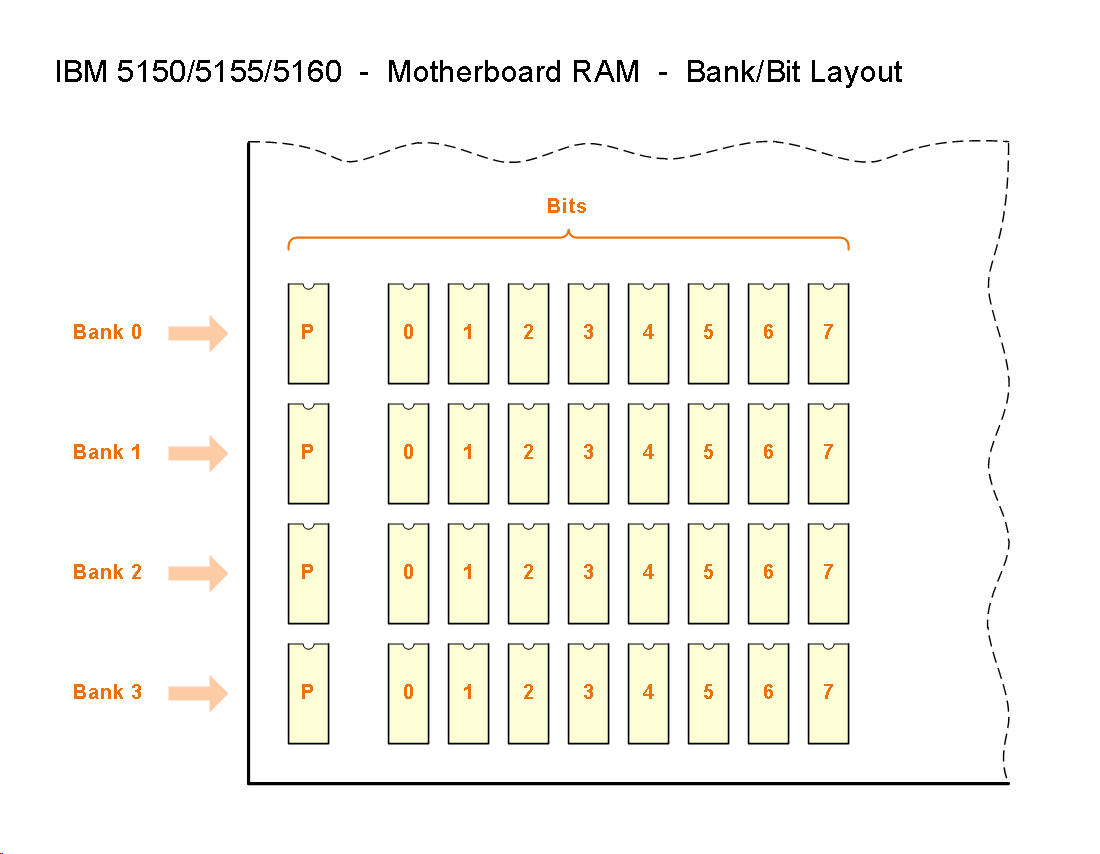
The IBM PC XT (5160) system board holds its RAM in four banks of nine chips, eight for the data bits and one for parity, and every bank is socketed.[1][2][3] Minuszerodegrees.net describes vintage RAM chips as having a relatively high failure rate.[4] A faulty chip on the XT does not always produce an error message: the way the XT's power-on self test (POST) sizes memory means a failed data chip often shows up only as less memory counted than is fitted.[4]
The repair finds the failed chip from the POST message, the memory count or a test program, and replaces it. The 5150's RAM guide covers the earlier machine, whose bank 0 is soldered.
Symptoms
[edit | edit source]- An error of the form aaaaa bb 201, for example 20000 80 201. aaaaa is the address of the fault and bb the failing bit or bits.[1][5]
- The memory count at the top left of the screen stops short of the memory fitted, with no error message. The POST writes to and reads from the first two addresses of each 64 KB block in turn and takes the first block that fails as the end of memory. Minuszerodegrees pulled a data chip from bank 3 of a 256 KB machine and it counted 192 KB with no 201 error. A failed parity chip, or some kinds of data chip failure, still give a 201.[4]
- A board that appears dead, with no picture, no beep and no drive activity. The POST tests the early RAM first and loops there if it fails: the first 16 KB with the 1982 BIOS, the first 64 KB with the 1986 BIOS. The dead-board symptom has many other causes; start with the minimum diagnostic configuration.[6]
- PARITY CHECK 1 is a parity error in system board RAM.[7]
Faults that look like failed RAM:
- A dirty SW1 switch 3 or 4, or a fault in the circuit that reads SW1, can also make the count stop short.[8]
- On the 256-640KB board, jumper E-2 must be fitted for the 256 KB chips in banks 0 and 1; without it the board counts only 256 KB.[9]
- A bit indicator with many bits set often means the POST tested RAM that is not there.[5]
- Minuszerodegrees saw 0C000 00 201 after fitting a 4164 by mistake in bank 0 of a 256-640KB board.[5]
Tools and parts
[edit | edit source]- An IC extractor, and a set of nine known-good RAM chips of the right type for the bank under test.[6][8]
- For a dead board: Ruud's diagnostic ROM in socket U18 with an MDA or CGA card, or a logic probe.[6]
- For a board that runs: DOS with DEBUG, Cassette BASIC, or CheckIt.[8]
| Board marking | Bank 0 | Bank 1 | Bank 2 | Bank 3 | Chip type |
|---|---|---|---|---|---|
| 64-256KB SYSTEM BOARD | 0 to 64 KB (00000 hex) | 64 to 128 KB (10000 hex) | 128 to 192 KB (20000 hex) | 192 to 256 KB (30000 hex) | 4164 in all banks, 200 ns or faster, pin 1 not connected |
| 256-640KB SYSTEM BOARD | 0 to 256 KB (00000 hex) | 256 to 512 KB (40000 hex) | 512 to 576 KB (80000 hex) | 576 to 640 KB | 41256 in banks 0 and 1, 4164 in banks 2 and 3, all 200 ns or faster, 4164 with pin 1 not connected |
Sources: minuszerodegrees.net.[1][2][8] The 200 ns figure is the one in IBM's Technical Reference for the 5160.[1]
Procedure
[edit | edit source]Identify the board
[edit | edit source]- Read the board marking: "64-256KB SYSTEM BOARD" is printed on the board; the 256-640KB board usually carries a label instead.[10]
- Check for a module at position U84. IBM notes that some boards in models 088, 089, 267, 277 and 278 are labelled 64Kb/256Kb although they are 256Kb/640Kb boards, and that a module at U84 identifies a 256/640 board.[9]
- Check SW1 switches 3 and 4. On the 5160 they enable the banks: both on enables bank 0 only, 3 off and 4 on banks 0 and 1, 3 on and 4 off banks 0 to 2, both off all four banks.[11]
Decode a 201 error
[edit | edit source]
- Convert the address aaaaa from hex to decimal and divide by 1024 to get KB. 30000 hex, for example, is 196,608, or 192 KB.[5]
- Find the bank that holds that address in the table above.[1][2]
- Read the bit from bb: 00 is the parity chip, and 01, 02, 04, 08, 10, 20, 40 and 80 are data bits 0 to 7. For any other value, write it in binary; each 1 is a failing bit.[5]
IBM's 1989 service manual describes the codes differently: four characters on the 64/256 board, the first giving the bank and the last two the bit (its example, 3040 201, is bank 3, bit 6), and seven characters on the 256/640 board, the first giving the bank and the sixth and seventh the bit (3C000 40 201 is bank 3, bit 6).[12] Minuszerodegrees, working with the 11/08/82 BIOS on the 64-256KB board, gives the five-and-two form shown above.[1]
Find the chip when there is no 201
[edit | edit source]When the count stops short, the first block not counted is the suspect. Minuszerodegrees' example is a 256-640KB board counting 512 KB instead of 640 KB, which points to bank 2, starting at 512 KB.[8]
- Flick SW1 switches 3 and 4 off and on a few times and return them to their setting.[8]
- Reseat all nine chips of the suspect bank.[8]
- Fit a known-good set of nine chips in the bank. Swapping one known-good chip into each position in turn also works, but does not catch two failed chips in the same bank.[8]
- Or test the bank in software. In DEBUG, enter
o a0 0to stop the board reacting to parity errors, thenf 8000:0 80 ffto fill the first 128 bytes of the bank at 512 KB with FF. Wait 10 seconds and enterd 8000:0. Repeat withf 8000:0 80 00. Any byte that reads back different from what was written shows the failing bit: in minuszerodegrees' example, 04 read back instead of 00 is bit 2.[8] - For another bank, use the segment of its start address: the hex address divided by 16, so 80000 hex is segment 8000.[8]
- Without DOS, boot to Cassette BASIC and run minuszerodegrees' program, which prints the combined failing bits at segment 8000 (change line 20 for another bank):[8]
10 out &hA0,0
20 def seg = &h8000 30 cbep = 0 40 poke 0,&hAA 50 cbep = cbep or (peek(0) xor &hAA) 60 poke 0,&h55 70 cbep = cbep or (peek(0) xor &h55) 80 poke 0,&hFF 90 cbep = cbep or (peek(0) xor &hFF) 100 poke 0,0 110 cbep = cbep or peek(0) 120 print hex$(cbep) run
- CheckIt's memory test, set to the address range of the suspect bank, reports the failing bits by address. It needs a minimum amount of working memory, so it may not run if the failed bank is a low one.[8]
The DEBUG and BASIC tests check the data chips only; they do not find a failed parity chip or a parity circuit fault.[8]
IBM's own method is to reduce the memory one bank at a time with the switches until the error stops, then put the switches back and swap the chips of the last bank removed until the error goes.[13]
Dead board: bank 0
[edit | edit source]Minuszerodegrees' procedure for a suspected bank 0 failure on the 5160:[6]
- If the board came to you faulty, check that every bank 0 chip is the right way round and of a type the board takes. On the 256-640KB board, bank 0 takes 41256 chips, not the 4164 used in banks 2 and 3.[6]
- Remove each bank 0 chip in turn, check that its pins are clean, complete and not bent under the chip, and refit it carefully, the right way round. A poor contact between a pin and its socket gives the same symptom as a failed chip.[6]
- Remove the chips from banks 1 to 3, leaving only bank 0.[6]
- Replace all nine bank 0 chips with a known-good set. Without one, use chips taken out in the previous step, of the correct type for bank 0.[6]
- Confirm that the fault really is in bank 0. With a logic probe, minuszerodegrees' checkpoint code page explains how to read the failing bit from activity on port A of the 8255. Ruud's diagnostic ROM in U18, with an MDA or CGA card, reports whether the first 64 KB is good. Minuszerodegrees does not recommend the Supersoft/Landmark ROM here, because it does not detect RAM addressing problems and can mislead on RAM errors.[6]

Replace the chip
[edit | edit source]- Switch off and unplug the machine, and open the system unit as described in the maintenance guide.
- Locate the chip from the bank and bit, using the layout diagram: each bank has the parity chip first, then bits 0 to 7.[3]
- Note which way round the chip is fitted, then lever it out with the extractor. The general method is in IC Removal and Socketing.
- Check the replacement against the table above, line up its pins and press it into the socket the same way round, making sure no pin folds under the chip.[6] IBM warns that a chip fitted the wrong way round can cause a memory error, a lock-up or a blank screen.[9]
- Refit the cards and cover, and set SW1 switches 3 and 4 for the banks fitted.[11]
Testing
[edit | edit source]- Switch on. IBM's normal sequence is a cursor after about four seconds, then the memory size in the top left corner counting up in 64 KB steps until all the memory has been tested, then one short beep.[14]
- Check that the count reaches the full amount fitted, with no 201 error.[4]
- Repeat whichever software test found the fault (DEBUG, BASIC or CheckIt) on the bank that was repaired.[8]
Board differences
[edit | edit source]- The 64-256KB board takes 4164 chips in all four banks and was supplied with the 11/08/82 BIOS. A documented modification lets it take 640 KB; see IBM PC XT Maintenance Guide#Identify your system board.[1][10]
- The 256-640KB board takes 41256 chips in banks 0 and 1 and 4164 chips in banks 2 and 3, and needs jumper E-2 to use the 41256 chips.[2][9]
- On both boards, memory on an expansion card can be added without filling the system board banks first, unlike the 5150.[1][2]
Related pages
[edit | edit source]- IBM PC XT (5160)
- IBM PC XT Troubleshooting Guide
- IBM PC XT Maintenance Guide
- IBM PC XT Capacitor Replacement Guide
- IBM PC (5150) RAM Replacement
- IBM Personal Computer Family Service Information Manual
- Logic Chip Testing
- IC Removal and Socketing
References
[edit | edit source]- ↑ 1.0 1.1 1.2 1.3 1.4 1.5 1.6 1.7 Minuszerodegrees.net, "IBM 5160: RAM on a '64 - 256KB' Type of Motherboard": four socketed banks of 4164 chips, 200 ns or faster with pin 1 not connected, the 200 ns figure in IBM's Technical Reference, bank addresses, the 201 format "aaaaa bb 201" with the example 20000 80 201 (11/08/82 BIOS), the halt on a fault in the first 16 KB, expansion card memory without filling the banks, and the 640 KB modification.
- ↑ 2.0 2.1 2.2 2.3 2.4 Minuszerodegrees.net, "IBM 5160: RAM on a '256 - 640KB' Type of Motherboard": 41256 chips in banks 0 and 1, 4164 chips in banks 2 and 3, 200 ns or faster, all socketed, and the halt on a fault in the first 64 KB (01/10/86 BIOS).
- ↑ 3.0 3.1 Minuszerodegrees.net, "IBM 5150/5155/5160 - Motherboard RAM - Bank/Bit Layout", diagram. Hosted here as File:IBM 5150 5160 system board RAM bank and bit layout (minuszerodegrees).jpg.
- ↑ 4.0 4.1 4.2 4.3 Minuszerodegrees.net, "IBM 5160 - Known Problems/Issues", sections "Flawed methodology for determining total conventional memory size" and "RAM failure in motherboard bank 0".
- ↑ 5.0 5.1 5.2 5.3 5.4 Minuszerodegrees.net, "IBM 5160 - Breakdown of 201 RAM Subsystem error", diagram with notes. Hosted here as File:IBM 5160 201 RAM error breakdown (minuszerodegrees).jpg.
- ↑ 6.00 6.01 6.02 6.03 6.04 6.05 6.06 6.07 6.08 6.09 Minuszerodegrees.net, "IBM 5160 - Faulty RAM in bank 0": the POST loop at checkpoint 4, early RAM by BIOS date, and the five-step procedure (inspection, reseating, isolation, substitution, logic probe or Ruud's diagnostic ROM in U18).
- ↑ Minuszerodegrees.net, "IBM 5160 - POST - Some errors": PARITY CHECK 1 and 2.
- ↑ 8.00 8.01 8.02 8.03 8.04 8.05 8.06 8.07 8.08 8.09 8.10 8.11 8.12 8.13 Minuszerodegrees.net, "IBM 5160" (identifying a faulty RAM chip when the count stops short): the 512 KB example, SW1 switches 3 and 4, reseating, a known-good set or a single known-good chip, CheckIt, the DEBUG commands, the Cassette BASIC program, Ruud's diagnostic ROM, and the limits of each.
- ↑ 9.0 9.1 9.2 9.3 IBM, Personal Computer Family Service Information Manual (1989), chapter 4, p. 4-7: chips plugged in wrong, the E-2 jumper for 256Kb modules in banks 0 and 1, and mislabelled 256Kb/640Kb boards identified by a module at U84.
- ↑ 10.0 10.1 Minuszerodegrees.net, "IBM 5160 - Motherboard Versions": the two board markings and the 640 KB modification.
- ↑ 11.0 11.1 Minuszerodegrees.net, "IBM 5160 - Motherboard Switch/Jumper Settings", switch block SW1, switches 3 and 4.
- ↑ IBM, Personal Computer Family Service Information Manual (1989), chapter 4, pp. 4-6 and 4-7: memory error codes for the 64Kb to 256Kb and 256Kb/640Kb system boards, with Figures 4-11 to 4-13.
- ↑ IBM, Personal Computer Family Service Information Manual (1989), chapter 4, p. 4-4: isolating a memory fault by reducing the memory one bank at a time and swapping modules in the failing bank.
- ↑ IBM, Personal Computer Family Service Information Manual, SA38-0037-00 (January 1989), chapter 4, p. 4-3: the power-on self test and the memory count in 64Kb increments. Hosted as File:IBM Personal Computer Family Service Information Manual SA38-0037-00.pdf.