

Panasonic FS-A1FM
 | |
| Panasonic FS-A1FM, with the floppy drive in the front edge. Photograph from the MSX Resource Center wiki; no freely licensed photograph has been found. | |
| Specifications | |
|---|---|
| Manufacturer | Matsushita Electric Industrial (Panasonic) |
| Type | MSX2 home computer with built-in modem |
| Released | 1988 (Japan) |
| Intro price | ¥89,800 |
| CPU | Z80A (in the Toshiba T9769 MSX-Engine) |
| Memory | 64 KB RAM, 8 KB SRAM, 128 KB video RAM |
| Storage | Built-in 3.5-inch 2DD floppy drive (720 KB), MSX cartridges, cassette |
| Display | Yamaha V9938 |
| Sound | PSG in the T9769 |
| Power | AC 100 V 50/60 Hz, 15 W |
| OS / Firmware | — |
| Predecessor | Panasonic FS-A1F |
| Model no. | FS-A1FM |
The Panasonic FS-A1FM is an MSX2 computer with a built-in modem, made by Matsushita Electric Industrial and sold in Japan from 1988 at ¥89,800. It follows the Panasonic FS-A1F, with the same built-in 3.5-inch floppy drive, and adds a 300/1200 bit/s modem with two modular telephone sockets, built-in communication software for The LINKS network, and 8 KB of SRAM used mainly by the modem software. It was sold in black.[1][2]
The MSX Resource Center describes the FS-A1FM as similar to the FS-A1F, and the two share a floppy drive, but the FS-A1FM's main board is a different design from the FS-A1F's. It is built round a Toshiba T9769 MSX-Engine in place of the FS-A1F's Yamaha S1985 and Zilog Z80, and even its DRAMs are in a different package.[1][3]
Hardware
[edit | edit source]The main board, printed "COPYRIGHT MATSUSHITA ELECTRIC IND. 1988", carries the Toshiba T9769 MSX-Engine (with the Z80A inside it), the Yamaha V9938 VDP, the Toshiba TC8566F floppy disk controller, an NEC gate array (μPD65013GF457), the system ROMs and the SRAM.[1][4] The photographed board shows the video and audio circuits on the main board itself, with no HIC-1 daughterboard of the kind fitted to the FS-A1F.[4]
The modem is on its own board, with a transformer and a relay for the telephone line, a USART and a PPI. A separate small board carries the two modular sockets and their surge protection.[5] The power supply is on a separate board inside the case and takes 100 V mains directly; the FS-A1FM is rated 15 W.[5][2] No circuit diagram of the FS-A1FM or its supply has been published.
The floppy drive is the same as the FS-A1F's, a belt-driven Matsushita unit, and takes the same belt: rubber, 0.3 mm thick, 58 mm in diameter and 3 mm wide.[1][6]
The main RAM can be taken to 128 KB by fitting two 64K × 4 DRAMs in ZIP packages (such as the MB81464-12) at IC17 and IC18, with 0.1 µF capacitors at C71 and C72, then shorting jumper J2 and cutting J3. The jumpers are between the VDP and the T9769. Without the jumper change the extra memory is not recognised.[3][1]
Backup cells
[edit | edit source]Two AA cells, type R6P (SUM-3), in a compartment in the base keep the clock and settings.[2] The MSX Resource Center recommends lithium cells or Eneloop rechargeables and advises against alkaline cells, which leak in time.[1]
Documentation
[edit | edit source]No Panasonic service manual for the FS-A1FM has been found. Its floppy drive is covered by the Panasonic FS-A1F General Maintenance guide.
Repair guides
[edit | edit source]- Panasonic FS-A1FM General Maintenance
- Panasonic FS-A1FM Troubleshooting Guide
- Panasonic FS-A1FM Capacitor Replacement Guide
Gallery
[edit | edit source]-
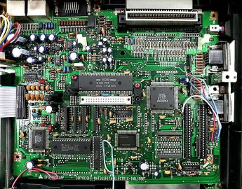 Main board, with the T9769 MSX-Engine at the right of the V9938
-
 Underside, with the rating label and the backup cell label


Related pages
[edit | edit source]References
[edit | edit source]- ↑ 1.0 1.1 1.2 1.3 1.4 1.5 Panasonic FS-A1FM, MSX Resource Center wiki, 7 March 2026—link(accessed 2026-10-21) Community page: similar to the FS-A1F with a built-in modem; first edition of the Toshiba T9769 MSX-Engine; Japan; black; 1988; ¥89,800; 64 KB RAM in slot 3-0 and 8 KB SRAM (NEC D4364CX-15L, mainly used by the modem software); 128 KB VRAM; V9938; PSG in the T9769; 720 KB drive; firmware switch, reset and pause buttons; modem with access to The LINKS network and MSX-Modem BASIC; kanji ROM level 1 and 12 × 12 dot kanji ROM; the firmware starts at boot and is skipped by holding DEL until a beep, which also deactivates the modem; the switch at the back skips the firmware without deactivating the modem; modem speed 300/1200 bit/s; Toshiba TC8566F floppy controller; RAM upgradable to 128 KB with two vertical MB81464-12 DRAMs (rare now) and two 100 nF capacitors, cutting jumper J3 and making J2, located between the VDP and the T9769; drive belt rubber, 0.3 mm thick, 58 mm diameter, 3 mm wide; connections include RF, composite video and audio, RGB, cassette, printer, two joystick ports, two cartridge slots and two RJ11 sockets; gallery captions "Panasonic FS-A1F/FS-A1FM drive", "FS-A1F/FS-A1FM drive PCB" and "Gate Array uPD65013GF457"; lithium or Eneloop backup cells recommended, alkaline advised against.
- ↑ 2.0 2.1 2.2 Underside of an FS-A1FM: rating label "MODEL NO. FS-A1FM, 電源入力 AC 100V 50/60Hz 15W, 松下電器産業株式会社, Part No. T0129ZA"; backup cell label giving R6P (SUM-3), two cells; telephone equipment approval label 認定番号 S88-3019-0. File:Panasonic FS-A1FM underside and rating label.jpg, from the MSX Resource Center wiki (uploaded by Mars2000you, 16 September 2020).
- ↑ 3.0 3.1 FS-A1FM MSX-ENGINEとメインRAM– up-c, 2011, updated 2022—link(accessed 2026-10-21) In Japanese. Under the T9769 MSX-Engine (written TC9769 on the page) are two 64K × 4 bit DRAMs in ZIP packages; two empty positions, IC17 and IC18, take two more, with 0.1 µF decoupling capacitors at C71 and C72; fitting the DRAMs and capacitors alone failed, because, unlike the FS-A1F upgrade, the board also needs jumper J2 shorted and J3 cut; the FS-A1F and FS-A1FM boards are completely different, and even the DRAM package differs.
- ↑ 4.0 4.1 File:Panasonic FS-A1FM main board.jpg, photograph uploaded to the MSX Resource Center wiki by Gdx on 11 December 2015: board printed "COPYRIGHT MATSUSHITA ELECTRIC IND. 1988", with the V9938, the T9769, the TC8566F at the lower left, a mask ROM printed DA534P66220, the NEC gate array, the modem connector CN9, and the video and audio circuits on the main board at the upper left.
- ↑ 5.0 5.1 FS-A1FM– up-c, 2011, updated 2022—link(accessed 2026-10-21) In Japanese. Specification table: Z80A 3.57 MHz, 64 KB main RAM, 128 KB VRAM (V9938), kanji ROM JIS level 1, PSG, one 3.5-inch 2DD drive, two slots, MSX-BASIC 2.0 and Disk BASIC 1.0, 1200 bit/s modem. Annotated photographs: power switch and power cable on the side; at the back, two modular sockets (line and telephone), RGB, printer, cassette, audio and video outputs, the built-in software on/off switch, the RF channel switch and RF output; inside, the floppy drive, the power supply board (電源基板), the RF module, and on the main board the VDP and VRAM, slot, FDC and ROM, gate array, MSX-Engine and main RAM areas; the modem board, with its transformer and relay, USART and PPI; the modular connector board, which carries little besides the sockets and a surge absorber.
- ↑ FS-A1Fの改造 前編– niga2—link(accessed 2026-10-21) In Japanese. The FS-A1F's built-in drive is a belt-driven Matsushita EME-212M; the drive connector pin-out is given for the "FS-A1F/FM".